I2C Control Registers
www.ti.com
1798
SPNU563A–March 2018
Submit Documentation Feedback
Copyright © 2018, Texas Instruments Incorporated
Inter-Integrated Circuit (I2C) Module
31.6.20 I2C Data Output Register (I2CDOUT)
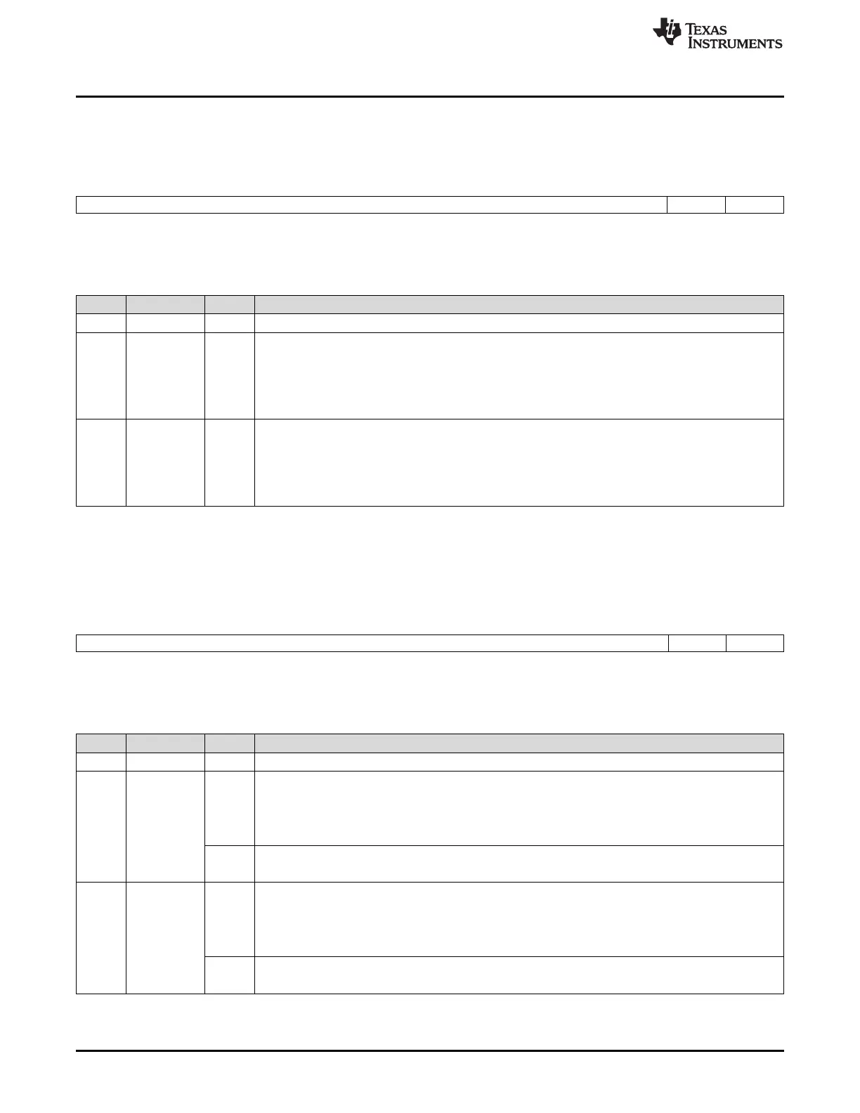
This register contains the values sent to the I2C pins. Figure 31-33 and Table 31-29 describe this register.
Figure 31-33. I2C Data Output Register (I2CDOUT) [offset 0x54]
15 2 1 0
Reserved SDAOUT SCLOUT
R-0 R/W-0 R/W-0
LEGEND: R/W = Read/Write; R = Read only; -n = value after reset
Table 31-29. I2C Data Output Register (I2CDOUT) Field Descriptions
Bit Field Value Description
15-2 Reserved 0 Reads return 0. Writes have no effect.
1 SDAOUT SDA data output.
This function is only active if the SDA pin is configured as an I/O pin with PINFUNC = 1. This bit
contains the value sent to the SDA pin.
0 The pin is driven low.
1 The pin is driven high.
0 SCLOUT SCL data output.
This function is only active if the SCL pin is configured as an I/O pin with PINFUNC = 1. This bit
contains the value sent to the SCL pin.
0 The pin is driven low.
1 The pin is driven high.
31.6.21 I2C Data Set Register (I2CDSET)
The I2CDSET register is an alias of the I2CDOUT register. Figure 31-34 and Table 31-30 describe this
register.
Figure 31-34. I2C Data Set Register (I2CDSET) [offset = 58h]
15 2 1 0
Reserved SDASET SCLSET
R-0 R/W-0 R/W-0
LEGEND: R/W = Read/Write; R = Read only; -n = value after reset
Table 31-30. I2C Data Set Register (I2CDSET) Field Description
Bit Field Value Description
15-2 Reserved 0 Reads return 0. Writes have no effect.
1 SDASET Serial data set.
This bit is used to set the SDA GPIO pin.
0 Read: Reads return value of SDAOUT.
Write: No effect.
1 Read: Reads return value of SDAOUT.
Write: SDAOUT is set to logic high (1).
0 SCLSET Serial clock set.
This bit is used to set the SCL GPIO pin.
0 Read: Reads return value of SCLOUT.
Write: No effect.
1 Read: Reads return value of SCLOUT.
Write: SCLOUT is set to logic high (1).

 Loading...


