I2C Control Registers
www.ti.com
1796
SPNU563A–March 2018
Submit Documentation Feedback
Copyright © 2018, Texas Instruments Incorporated
Inter-Integrated Circuit (I2C) Module
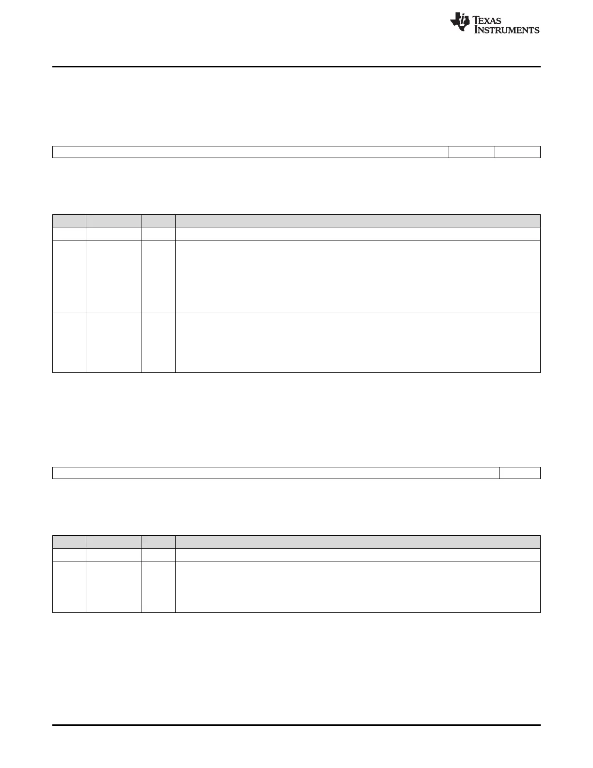
31.6.16 I2C DMA Control Register (I2CDMACR)
This register contains the transmit and receive DMA enable bits. Figure 31-29 and Table 31-25 describe
this register.
Figure 31-29. I2C DMA Control Register (I2CDMACR) [offset = 3Ch]
15 2 1 0
Reserved TXDMAEN RXDMAEN
R-0 R/W-1 R/W-1
LEGEND: R/W = Read/Write; R = Read only; -n = value after reset
Table 31-25. I2C DMA Control Register (I2CDMACR) Field Descriptions
Bit Field Value Description
15-2 Reserved 0 Reads return 0. Writes have no effect.
1 TXDMAEN Transmitter DMA enable.
This bit controls the transmit DMA event pin to the system. When this bit is a 1, the DMA transmit event
is enabled and the DMA can occur. When this bit is a 0, the DMA transmit event is disabled.
Writing a 1 to this bit will send a TXDMA request to the DMA module, if PINFUNC is also cleared to 0.
0 The transmit DMA is disabled.
1 The transmit DMA is enabled.
0 RXDMAEN Receive DMA enable.
This bit controls the receive DMA event pin to the system. When this bit is 1, the DMA receive event is
enabled and the DMA can occur. When this bit is a 0, the DMA receive event is disabled.
0 The receive DMA is disabled.
1 The receive DMA is enabled.
31.6.17 I2C Pin Function Register (I2CPFNC)
Figure 31-30 and Table 31-26 describe this register.
Figure 31-30. I2C Pin Function Register (I2CPFNC) [offset = 48h]
15 1 0
Reserved PINFUNC
R-0 R/W-0
LEGEND: R/W = Read/Write; R = Read only; -n = value after reset
Table 31-26. I2C Pin Function Register (I2CPFNC) Field Descriptions
Bit Field Value Description
15-1 Reserved 0 Reads return 0. Writes have no effect.
0 PINFUNC SDA and SCL pin function.
This bit controls whether the SDA and SCL pins function as I2C pins or as I/O pins.
0 SDA and SCL pins function as I2C pins.
1 SDA and SCL pins function as I/O pins.

 Loading...


