System and Peripheral Control Registers
www.ti.com
180
SPNU563A–March 2018
Submit Documentation Feedback
Copyright © 2018, Texas Instruments Incorporated
Architecture
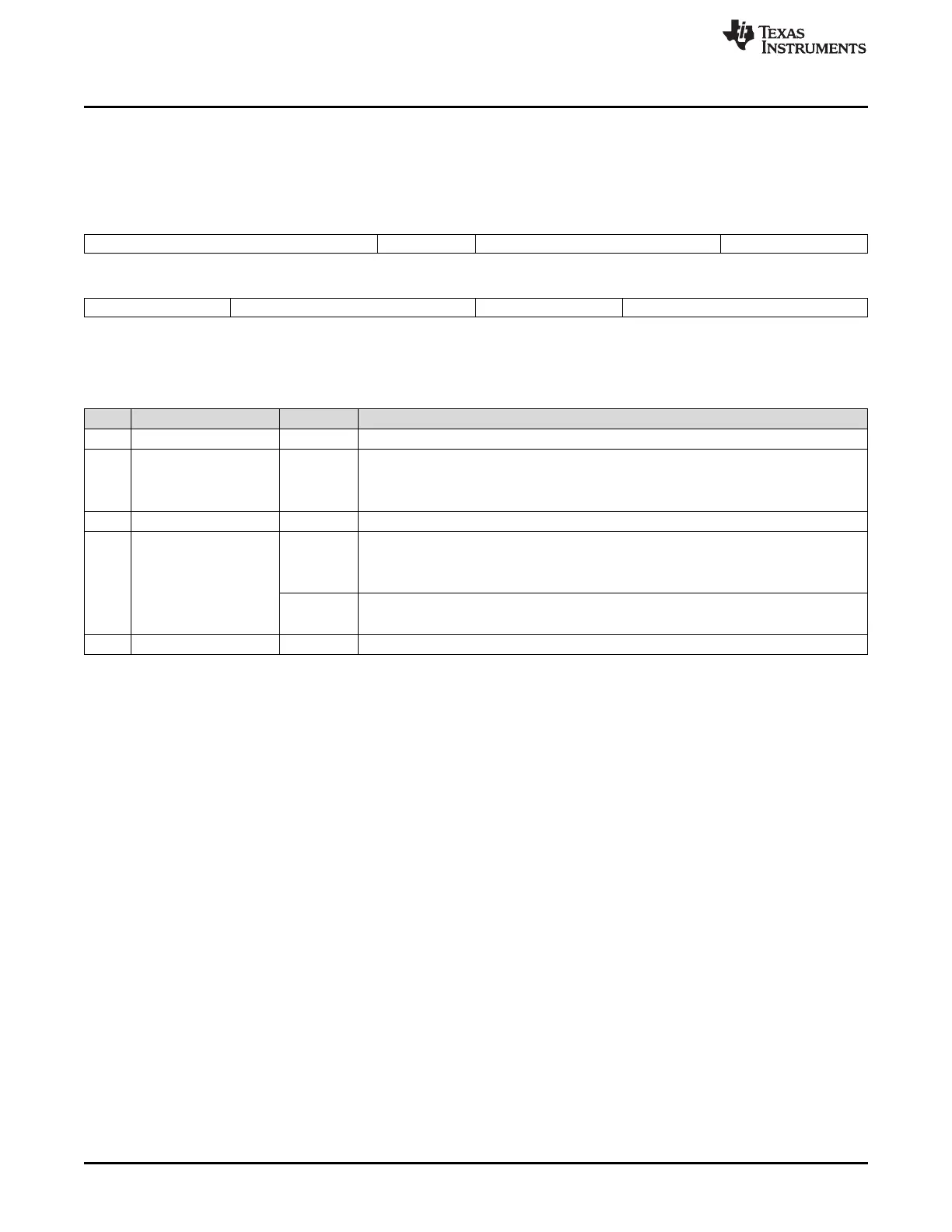
2.5.1.30 LPO/Clock Monitor Control Register (LPOMONCTL)
The LPOMONCTL register, shown in Figure 2-37 and described in Table 2-49, controls the Low
Frequency (Clock Source 4) and High Frequency (Clock Source 5) Low Power Oscillator's trim values.
Figure 2-37. LPO/Clock Monitor Control Register (LPOMONCTL) (offset = 088h)
31 25 24 23 17 16
Reserved BIAS ENABLE Reserved OSCFRQCONFIGCNT
R-0 R/WP-1 R-0 R/WP-0
15 13 12 8 7 5 4 0
Reserved HFTRIM Reserved LFTRIM
R-0 R/WP-10h R-0 R/WP-10h
LEGEND: R/W = Read/Write; R = Read only; WP = Write in privileged mode only; -n = value after reset
Table 2-49. LPO/Clock Monitor Control Register (LPOMONCTL) Field Descriptions
Bit Field Value Description
31-25 Reserved 0 Reads return 0. Writes have no effect.
24 BIAS ENABLE Bias enable.
0 The bias circuit inside the low-power oscillator (LPO) is disabled.
1 The bias circuit inside the low-power oscillator (LPO) is enabled.
23-17 Reserved 0 Reads return 0. Writes have no effect.
16 OSCFRQCONFIGCNT Configures the counter based on OSC frequency.
0 Read: OSC freq is ≤ 20MHz.
Write: A write of 0 has no effect.
1 Read: OSC freq is > 20MHz and ≤ 80MHz.
Write: A write of 1 has no effect.
15-13 Reserved 0 Reads return 0. Writes have no effect.

 Loading...


