www.ti.com
System and Peripheral Control Registers
233
SPNU563A–March 2018
Submit Documentation Feedback
Copyright © 2018, Texas Instruments Incorporated
Architecture
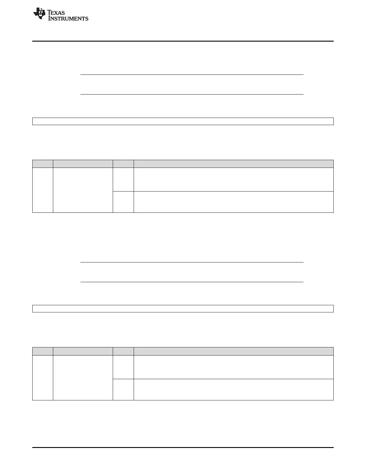
2.5.3.18 Peripheral Power-Down Set Register 1 (PSPWRDWNSET1)
There is one bit for each quadrant for PS8 to PS15. The protection scheme is described in
Section 2.5.3.17. This register is shown in Figure 2-89 and described in Table 2-103.
NOTE: Only those bits that have a slave at the corresponding bit position are implemented. Writes
to unimplemented bits have no effect and reads are 0.
Figure 2-89. Peripheral Power-Down Set Register 1 (PSPWRDWNSET1) (offset = 84h)
31 0
PS[15-8]QUAD[3-0]PWRDWNSET
R/WP-1
LEGEND: R/W = Read/Write; WP = Write in privileged mode only; -n = value after reset
Table 2-103. Peripheral Power-Down Set Register 1 (PSPWRDWNSET1) Field Descriptions
Bit Field Value Description
31-0 PS[15-8]QUAD[3-0]
PWRDWNSET
Peripheral select quadrant clock power-down set.
0 Read: The clock to the peripheral select quadrant is active.
Write: The bit is unchanged.
1 Read: The clock to the peripheral select quadrant is inactive.
Write: The corresponding bit in PSPWRDWNSET1 and PSPWRDWNCLR1 registers is set
to 1.
2.5.3.19 Peripheral Power-Down Set Register 2 (PSPWRDWNSET2)
There is one bit for each quadrant for PS16 to PS23. The protection scheme is described in
Section 2.5.3.17. This register is shown in Figure 2-90 and described in Table 2-104.
NOTE: Only those bits that have a slave at the corresponding bit position are implemented. Writes
to unimplemented bits have no effect and reads are 0.
Figure 2-90. Peripheral Power-Down Set Register 2 (PSPWRDWNSET2) (offset = 88h)
31 0
PS[23-16]QUAD[3-0]PWRDWNSET
R/WP-1
LEGEND: R/W = Read/Write; WP = Write in privileged mode only; -n = value after reset
Table 2-104. Peripheral Power-Down Set Register 2 (PSPWRDWNSET2) Field Descriptions
Bit Field Value Description
31-0 PS[23-16]QUAD[3-0]
PWRDWNSET
Peripheral select quadrant clock power-down set.
0 Read: The clock to the peripheral select quadrant is active.
Write: The bit is unchanged.
1 Read: The clock to the peripheral select quadrant is inactive.
Write: The corresponding bit in PSPWRDWNSET2 and PSPWRDWNCLR2 registers is set
to 1.

 Loading...


