www.ti.com
Control Registers and Control Packets
791
SPNU563A–March 2018
Submit Documentation Feedback
Copyright © 2018, Texas Instruments Incorporated
Direct Memory Access Controller (DMA) Module
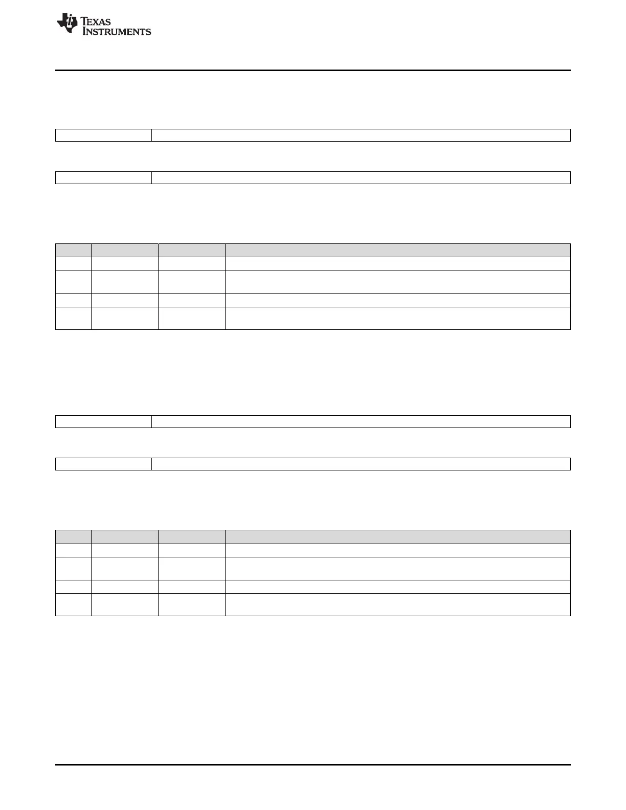
20.3.2.5 Element Index Offset Register (EIOFF)
Figure 20-114. Element Index Offset Register (EIOFF) [offset = 14h]
31 29 28 16
Reserved EIDXD
R-X R/WP-X
15 13 12 0
Reserved EIDXS
R-X R/WP-X
LEGEND: R/W = Read/Write; R = Read only; WP = Write in privilege mode only; X = value is unknown; -n = value after reset
Table 20-104. Element Index Offset Register (EIOFF) Field Descriptions
Bit Field Value Description
31-29 Reserved 0 Reads are undefined. Writes have no effect.
28-16 EIDXD 0-1FFFh Destination address element index. These bits define the offset to be added to the
destination address after each element transfer.
15-13 Reserved 0 Reads are undefined. Writes have no effect.
12-0 EIDXS 0-1FFFh Source address element index. These bits define the offset to be added to the source
address after each element transfer.
20.3.2.6 Frame Index Offset Register (FIOFF)
Figure 20-115. Frame Index Offset Register (FIOFF) [offset = 18h]
31 29 28 16
Reserved FIDXD
R-X R/WP-X
15 13 12 0
Reserved FIDXS
R-X R/WP-X
LEGEND: R/W = Read/Write; R = Read only; WP = Write in privilege mode only; X = value is unknown; -n = value after reset
Table 20-105. Frame Index Offset Register (FIOFF) Field Descriptions
Bit Field Value Description
31-29 Reserved 0 Reads are undefined. Writes have no effect.
28-16 FIDXD 0-1FFFh Destination address frame index. These bits define the offset to be added to the destination
address after element count reached 1.
15-13 Reserved 0 Reads are undefined. Writes have no effect.
12-0 FIDXS 0-1FFFh Source address frame index. These bits define the offset to be added to the source address
after element count reached 1.

 Loading...


