ADC Registers
www.ti.com
916
SPNU563A–March 2018
Submit Documentation Feedback
Copyright © 2018, Texas Instruments Incorporated
Analog To Digital Converter (ADC) Module
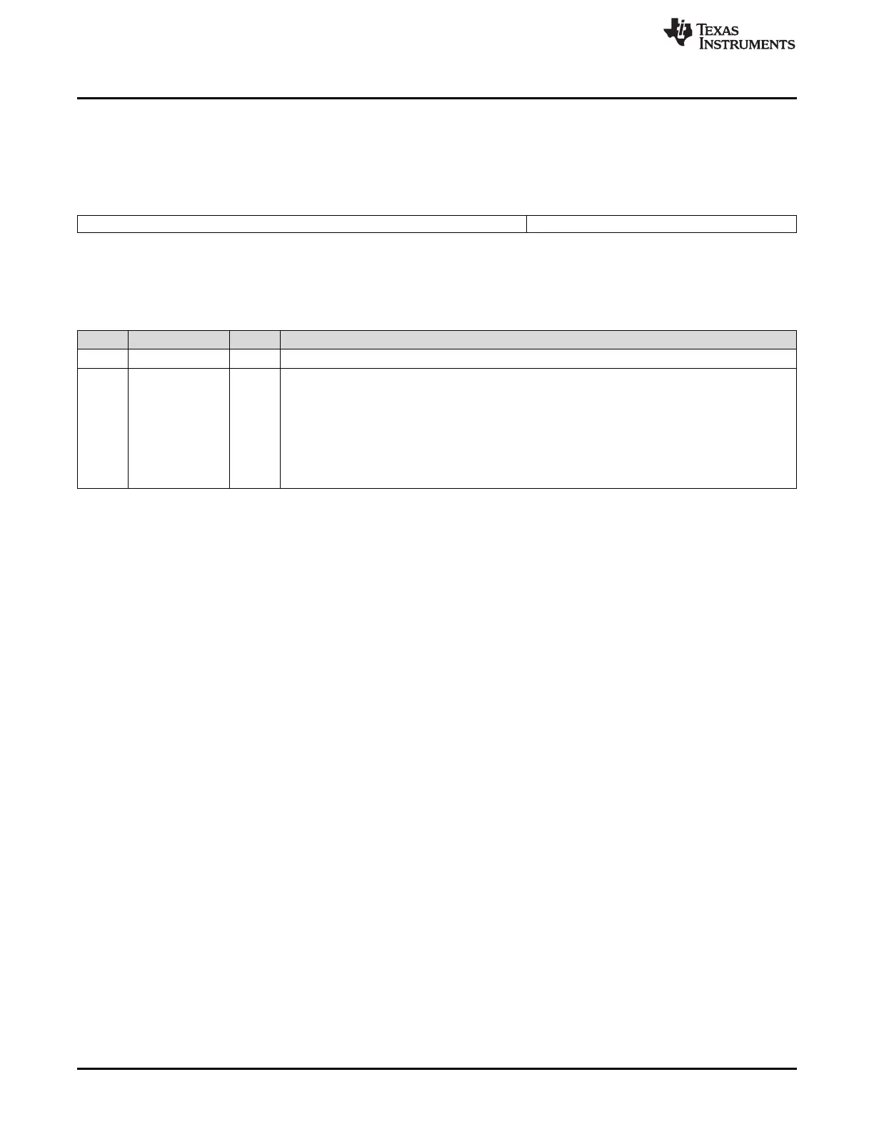
22.3.27 ADC Group2 Sampling Time Configuration Register (ADG2SAMP)
ADC Group2 Sampling Time Configuration Register (ADG2SAMP) is shown in Figure 22-49 and
described in Table 22-33.
Figure 22-49. ADC Group2 Sampling Time Configuration Register (ADG2SAMP) [offset = 68h]
31 12 11 0
Reserved G2_ACQ
R-0 R/W-0
LEGEND: R/W = Read/Write; R = Read only; -n = value after reset
Table 22-33. ADC Group2 Sampling Time Configuration Register (ADG2SAMP)
Field Descriptions
Bit Field Value Description
31-12 Reserved 0 Reads return 0. Writes have no effect.
11-0 G2_ACQ Group2 Acquisition Time. These bits define the sampling window (SW) for the Group2 conversions.
SW = G2_ACQ + 2 in terms of ADCLK cycles.
There are two factors that determine the minimum sampling window value required:
First, the ADC module design requires that SW >= 3 ADCLK cycles.
Second, the ADC input impedance necessitates a certain minimum sampling time. This needs to be
assured by configuring the G2_ACQ value properly considering the frequency of the ADCLK signal.
Refer to the device datasheet to determine the minimum sampling time for this device.

 Loading...


