www.ti.com
System and Peripheral Control Registers
153
SPNU563A–March 2018
Submit Documentation Feedback
Copyright © 2018, Texas Instruments Incorporated
Architecture
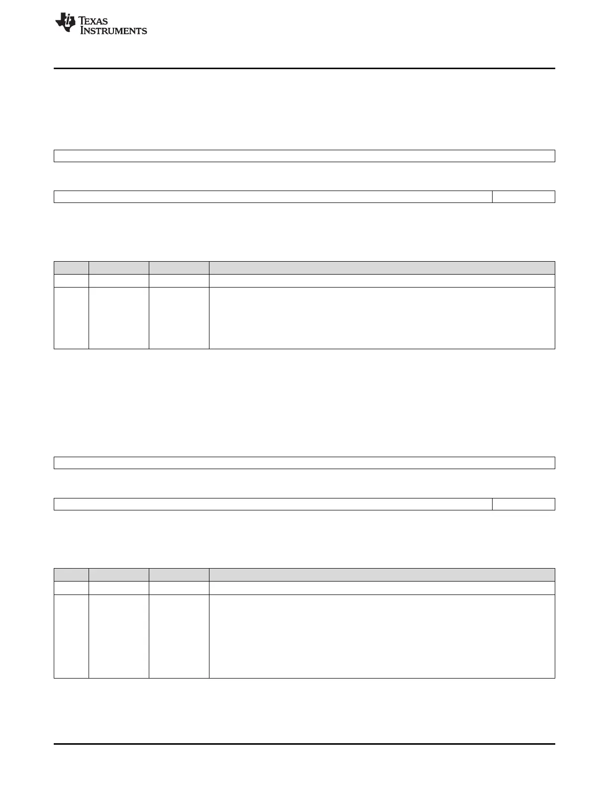
2.5.1.1 SYS Pin Control Register 1 (SYSPC1)
The SYSPC1 register, shown in Figure 2-8 and described in Table 2-19, controls the function of the ECLK
pin.
Figure 2-8. SYS Pin Control Register 1 (SYSPC1) (offset = 00h)
31 16
Reserved
R-0
15 1 0
Reserved ECPCLKFUN
R-0 R/W-0
LEGEND: R/W = Read/Write; R = Read only; -n = value after reset
Table 2-19. SYS Pin Control Register 1 (SYSPC1) Field Descriptions
Bit Field Value Description
31-1 Reserved 0 Reads return 0. Writes have no effect.
0 ECPCLKFUN ECLK function. This bit changes the function of the ECLK pin.
0 ECLK is in GIO mode.
1 ECLK is in functional mode as a clock output.
Note: Proper ECLK duty cycle is not guaranteed until 1 ECLK cycle has elapsed after
switching into functional mode.
2.5.1.2 SYS Pin Control Register 2 (SYSPC2)
The SYSPC2 register, shown in Figure 2-9 and described in Table 2-20, controls whether the pin is an
input or an output when in GIO mode.
Figure 2-9. SYS Pin Control Register 2 (SYSPC2) (offset = 04h)
31 16
Reserved
R-0
15 1 0
Reserved ECPCLKDIR
R-0 R/W-0
LEGEND: R/W = Read/Write; R = Read only; -n = value after reset
Table 2-20. SYS Pin Control Register 2 (SYSPC2) Field Descriptions
Bit Field Value Description
31-1 Reserved 0 Reads return 0. Writes have no effect.
0 ECPCLKDIR ECLK data direction. This bit controls the direction of the ECLK pin when it is configured to be
in GIO mode only.
0 The ECLK pin is an input.
Note: If the pin direction is set as an input, the output buffer is tristated.
1 The ECLK pin is an output.
Note: The ECLK pin is placed into GIO mode by clearing the ECPCLKFUN bit to 0 in the
SYSPC1 register.

 Loading...


