System and Peripheral Control Registers
www.ti.com
154
SPNU563A–March 2018
Submit Documentation Feedback
Copyright © 2018, Texas Instruments Incorporated
Architecture
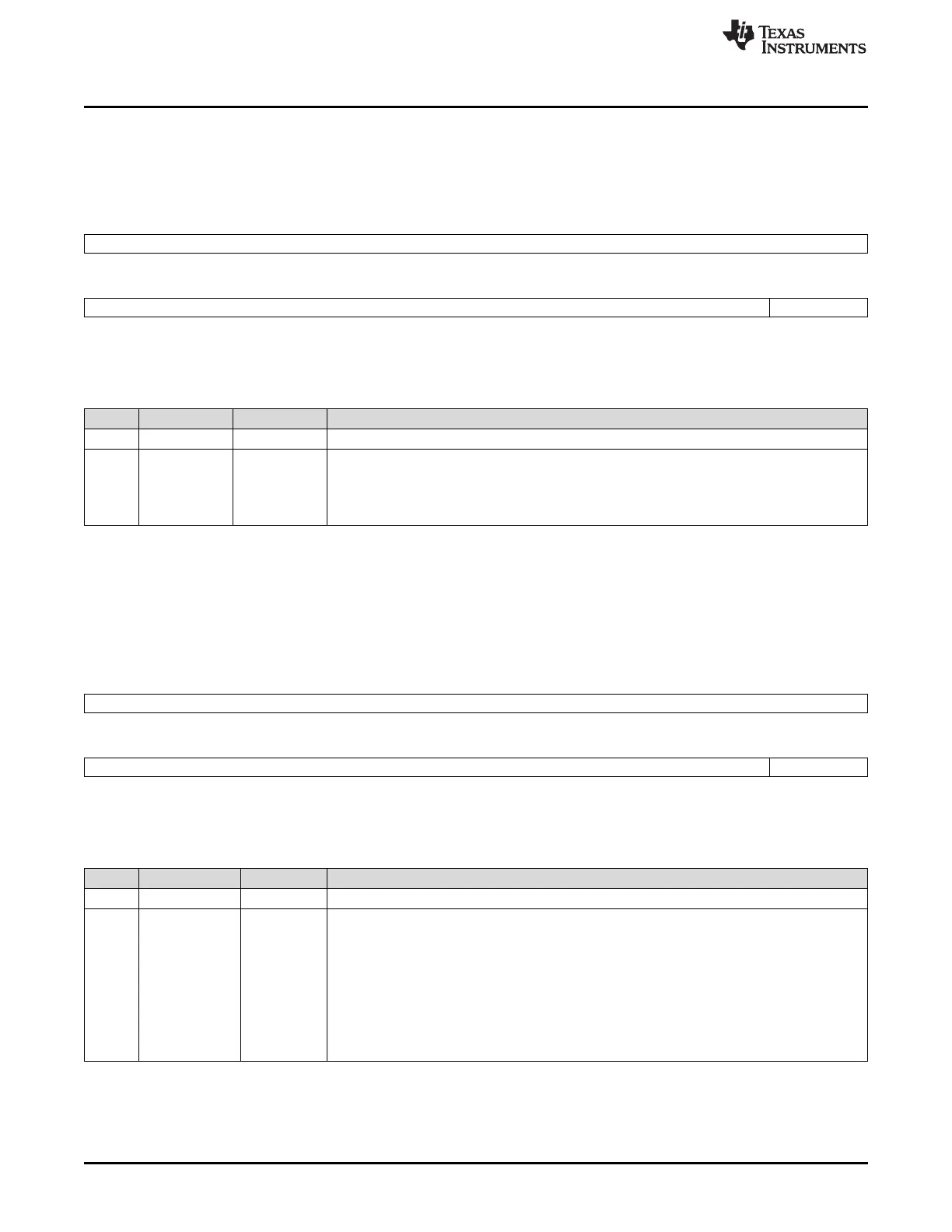
2.5.1.3 SYS Pin Control Register 3 (SYSPC3)
The SYSPC3 register, shown in Figure 2-10 and described in Table 2-21, displays the logic state of the
ECLK pin when it is in GIO mode.
Figure 2-10. SYS Pin Control Register 3 (SYSPC3) (offset = 08h)
31 16
Reserved
R-0
15 1 0
Reserved ECPCLKDIN
R-0 R-U
LEGEND: R = Read only; U = value is undefined; -n = value after reset
Table 2-21. SYS Pin Control Register 3 (SYSPC3) Field Descriptions
Bit Field Value Description
31-1 Reserved 0 Reads return 0. Writes have no effect.
0 ECPCLKDIN ECLK data in. This bit displays the logic state of the ECLK pin when it is configured to be in
GIO mode.
0 The ECLK pin is at logic low (0).
1 The ECLK pin is at logic high (1).
2.5.1.4 SYS Pin Control Register 4 (SYSPC4)
The SYSPC4 register, shown in Figure 2-11 and described in Table 2-22, controls the logic level output
function of the ECLK pin when it is configured as an output in GIO mode.
Figure 2-11. SYS Pin Control Register 4 (SYSPC4) (offset = 0Ch)
31 16
Reserved
R-0
15 1 0
Reserved ECPCLKDOUT
R-0 R/W-0
LEGEND: R/W = Read/Write; R = Read only; -n = value after reset
Table 2-22. SYS Pin Control Register 4 (SYSPC4) Field Descriptions
Bit Field Value Description
31-1 Reserved 0 Reads return 0. Writes have no effect.
0 ECPCLKDOUT ECLK data out write. This bit is only active when the ECLK pin is configured to be in GIO mode.
Writes to this bit will only take effect when the ECLK pin is configured as an output in GIO
mode. The current logic state of the ECLK pin will be displayed by this bit in both input and
output GIO mode.
0 The ECLK pin is driven to logic low (0).
1 The ECLK pin is driven to logic high (1).
Note: The ECLK pin is placed into GIO mode by clearing the ECPCLKFUN bit to 0 in the
SYSPC1 register. The ECLK pin is placed in output mode by setting the ECPCLKDIR bit
to 1 in the SYSPC2 register.

 Loading...


