www.ti.com
System and Peripheral Control Registers
159
SPNU563A–March 2018
Submit Documentation Feedback
Copyright © 2018, Texas Instruments Incorporated
Architecture
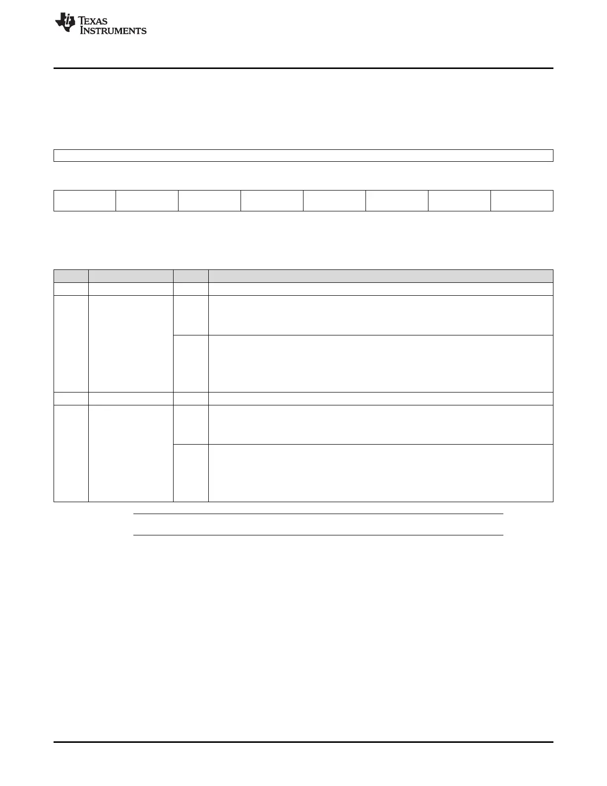
2.5.1.11 Clock Source Disable Set Register (CSDISSET)
The CSDISSET register, shown in Figure 2-18 and described in Table 2-30, sets clock sources to the
disabled state.
Figure 2-18. Clock Source Disable Set Register (CSDISSET) (offset = 34h)
31 8
Reserved
R-0
7 6 5 4 3 2 1 0
SETCLKSR7
OFF
SETCLKSR6
OFF
SETCLKSR5
OFF
SETCLKSR4
OFF
SETCLKSR3
OFF
Reserved SETCLKSR1
OFF
SETCLKSR0
OFF
R/WP-1 R/WP-1 R/WP-0 R/WP-0 R/WP-1 R-1 R/WP-1 R/WP-0
LEGEND: R/W = Read/Write; R = Read only; WP = Write in privileged mode only; -n = value after reset
Table 2-30. Clock Source Disable Set Register (CSDISSET) Field Descriptions
Bit Field Value Description
31-8 Reserved 0 Reads return 0. Writes have no effect.
7-3 SETCLKSR[7-3]OFF Set clock source[7-3] to the disabled state.
0 Read: Clock source[7-3] is enabled.
Write: Clock source[7-3] is unchanged.
1 Read: Clock source[7-3] is disabled.
Write: Clock source[7-3] is set to the disabled state.
Note: After a new clock source disable bit is set via the CSDISSET register, the new
status of the bit will be reflected in the CSDIS register (offset 30h), the CSDISSET
register (offset 34h), and the CSDISCLR register (offset 38h).
2 Reserved 1 Reads return 1. Writes have no effect.
1-0 SETCLKSR[1-0]OFF Set clock source[1-0] to the disabled state.
0 Read: Clock source[1-0] is enabled.
Write: Clock source[1-0] is unchanged.
1 Read: Clock source[1-0] is disabled.
Write: Clock source[1-0] is set to the disabled state.
Note: After a new clock source disable bit is set via the CSDISSET register, the new
status of the bit will be reflected in the CSDIS register (offset 30h), the CSDISSET
register (offset 34h), and the CSDISCLR register (offset 38h).
NOTE: A list of the available clock sources is shown in the Table 2-29.

 Loading...


