www.ti.com
SCI/LIN Control Registers
1699
SPNU563A–March 2018
Submit Documentation Feedback
Copyright © 2018, Texas Instruments Incorporated
Serial Communication Interface (SCI)/ Local Interconnect Network (LIN)
Module
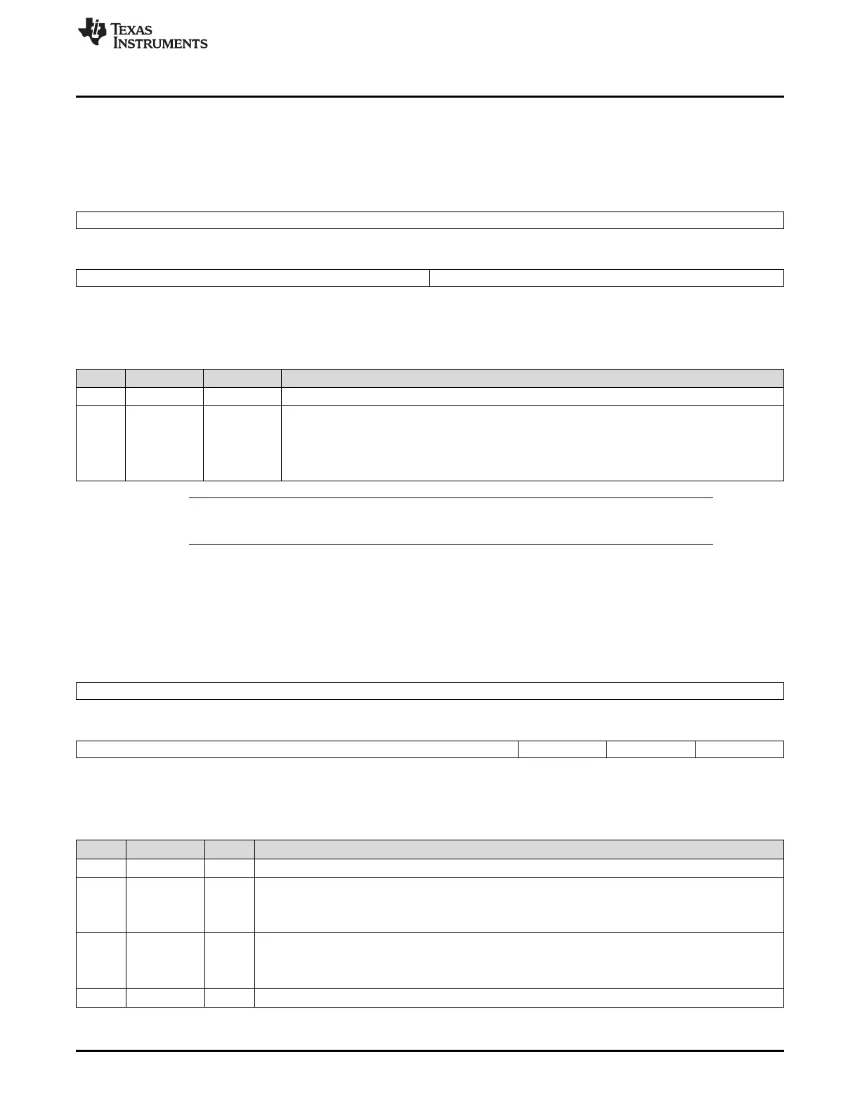
29.7.13.3 Transmit Data Buffer Register (SCITD)
Data to be transmitted is written to the SCITD register. Figure 29-42 and Table 29-28 illustrate this
register.
Figure 29-42. Transmit Data Buffer Register (SCITD) (offset = 38h)
31 16
Reserved
R-0
15 8 7 0
Reserved TD
R-0 R/W-0
LEGEND: R/W = Read/Write; R = Read only; -n = value after reset
Table 29-28. Transmit Data Buffer Register (SCITD) Field Descriptions
Bit Field Value Description
31-8 Reserved 0 Reads return 0. Writes have no effect.
7-0 TD 0-FFh Transmit data. This bit is effective in SCI-compatible mode only. Data to be transmitted is written
to the SCITD register. The transfer of data from this register to the transmit shift register
SCITXSHF sets the TXRDY flag, which indicates that SCITD is ready to be loaded with another
byte of data.
Note: If SET TX INT is set, this data transfer also causes an interrupt.
NOTE: Data written to the SCITD register that is fewer than eight bits long must be right justified, but
it does not need to be padded with leading zeros.
29.7.14 SCI Pin I/O Control Register 0 (SCIPIO0)
Figure 29-43 and Table 29-29 illustrate this register.
Figure 29-43. SCI Pin I/O Control Register 0 (SCIPIO0) (offset = 3Ch)
31 8
Reserved
R-0
7 3 2 1 0
Reserved TX FUNC RX FUNC Reserved
R-0 R/W-0 R/W-0 R/W-0
LEGEND: R/W = Read/Write; R = Read only; -n = value after reset
Table 29-29. SCI Pin I/O Control Register 0 (SCIPIO0) Field Descriptions
Bit Field Value Description
31-3 Reserved 0 Reads return 0. Writes have no effect.
2 TX FUNC Transfer function. This bit is effective in LIN or SCI mode. This bit defines the function of pin LINTX.
0 LINTX is a general-purpose digital I/O pin.
1 LINTX is the SCI/LIN transmit pin.
1 RX FUNC Receive function. This bit is effective in LIN or SCI mode. This bit defines the function of pin LINRX.
0 LINRX is a general-purpose digital I/O pin.
1 LINRX is the SCI/LIN receive pin.
0 Reserved 0 Writes have no effect.

 Loading...


