www.ti.com
SCI/LIN Control Registers
1701
SPNU563A–March 2018
Submit Documentation Feedback
Copyright © 2018, Texas Instruments Incorporated
Serial Communication Interface (SCI)/ Local Interconnect Network (LIN)
Module
29.7.16 SCI Pin I/O Control Register 2 (SCIPIO2)
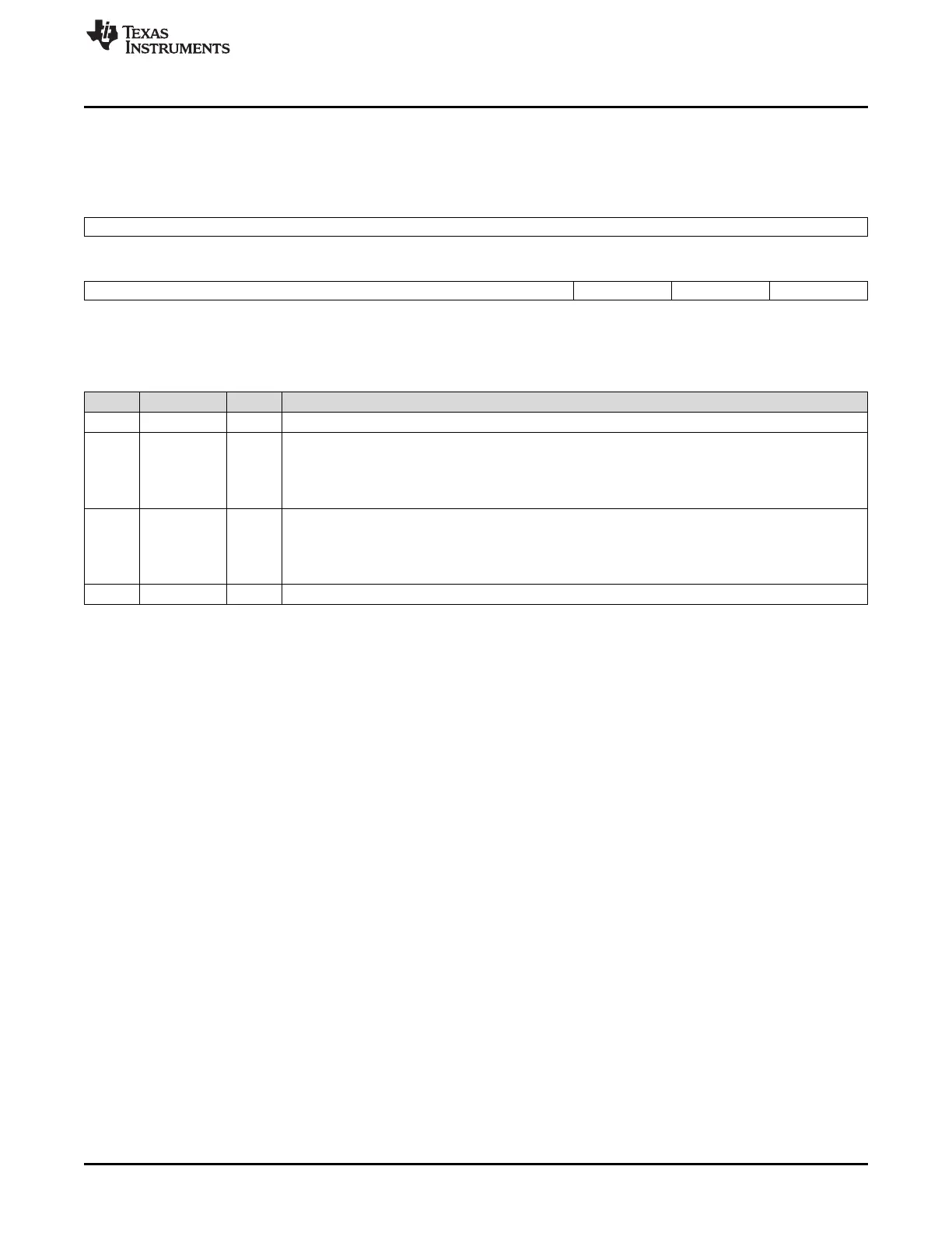
Figure 29-45 and Table 29-33 illustrate this register.
Figure 29-45. SCI Pin I/O Control Register 2 (SCIPIO2) (offset = 44h)
31 8
Reserved
R-0
7 3 2 1 0
Reserved TX IN RX IN Reserved
R-0 R-X R-X R-X
LEGEND: R = Read only; X= value is indeterminate; -n = value after reset
Table 29-33. SCI Pin I/O Control Register 2 (SCIPIO2) Field Descriptions
Bit Field Value Description
31-3 Reserved 0 Reads return 0. Writes have no effect.
2 TX IN Transmit pin in. This bit is effective in LIN or SCI mode. This bit contains the current value on the LINTX
pin.
0 The LINTX pin is at logic low (0).
1 The LINTX pin is at logic high (1).
1 RX IN Receive pin in. This bit is effective in LIN or SCI mode. This bit contains the current value on the LINRX
pin.
0 The LINRX pin is at logic low (0).
1 The LINRX pin is at logic high (1).
0 Reserved 0 Writes have no effect.

 Loading...


