ePWM Registers
www.ti.com
2082
SPNU563A–March 2018
Submit Documentation Feedback
Copyright © 2018, Texas Instruments Incorporated
Enhanced Pulse Width Modulator (ePWM) Module
35.4.4 Dead-Band Submodule Registers
35.4.4.1 Dead-Band Generator Control Register (DBCTL)
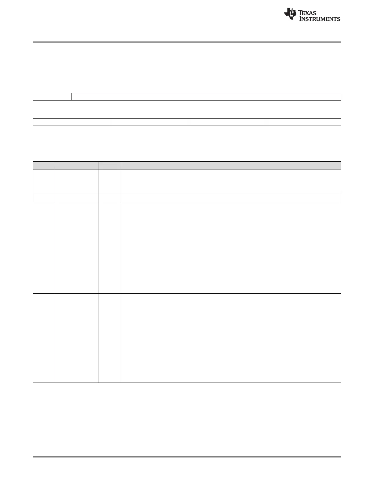
Figure 35-75. Dead-Band Generator Control Register (DBCTL) [offset = 1Ch]
15 14 8
HALFCYCLE Reserved
R/W-0 R-0
7 6 5 4 3 2 1 0
Reserved IN_MODE POLSEL OUT_MODE
R-0 R/W-0 R/W-0 R/W-0
LEGEND: R/W = Read/Write; R = Read only; -n = value after reset
Table 35-35. Dead-Band Generator Control Register (DBCTL) Field Descriptions
Bits Name Value Description
15 HALFCYCLE Half Cycle Clocking Enable Bit.
0 Full cycle clocking enabled. The dead-band counters are clocked at the TBCLK rate.
1 Half cycle clocking enabled. The dead-band counters are clocked at TBCLK × 2.
14-6 Reserved 0 Reserved
5-4 IN_MODE Dead Band Input Mode Control.
Bit 5 controls the S5 switch and bit 4 controls the S4 switch shown in Figure 35-28.
This allows you to select the input source to the falling-edge and rising-edge delay.
To produce classical dead-band waveforms the default is EPWMxA In is the source for both falling
and rising-edge delays.
0 EPWMxA In (from the action-qualifier) is the source for both falling-edge and rising-edge delay.
1h EPWMxB In (from the action-qualifier) is the source for rising-edge delayed signal.
EPWMxA In (from the action-qualifier) is the source for falling-edge delayed signal.
2h EPWMxA In (from the action-qualifier) is the source for rising-edge delayed signal.
EPWMxB In (from the action-qualifier) is the source for falling-edge delayed signal.
3h EPWMxB In (from the action-qualifier) is the source for both rising-edge delay and falling-edge
delayed signal.
3-2 POLSEL Polarity Select Control.
Bit 3 controls the S3 switch and bit 2 controls the S2 switch shown in Figure 35-28.
This allows you to selectively invert one of the delayed signals before it is sent out of the dead-band
submodule.
The following descriptions correspond to classical upper/lower switch control as found in one leg of
a digital motor control inverter.
These assume that DBCTL[OUT_MODE] = 1,1 and DBCTL[IN_MODE] = 0,0. Other enhanced
modes are also possible, but not regarded as typical usage modes.
0 Active high (AH) mode. Neither EPWMxA nor EPWMxB is inverted (default).
1h Active low complementary (ALC) mode. EPWMxA is inverted.
2h Active high complementary (AHC). EPWMxB is inverted.
3h Active low (AL) mode. Both EPWMxA and EPWMxB are inverted.

 Loading...


