www.ti.com
Control Registers and Control Packets
749
SPNU563A–March 2018
Submit Documentation Feedback
Copyright © 2018, Texas Instruments Incorporated
Direct Memory Access Controller (DMA) Module
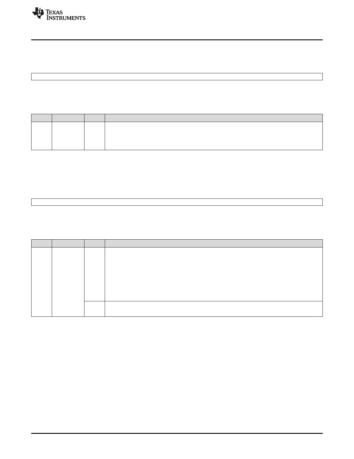
20.3.1.37 Global Interrupt Flag Register (GINTFLAG)
Figure 20-55. Global Interrupt Flag Register (GINTFLAG) [offset = 11Ch]
31 0
GINT[31:0]
R/WP-0
LEGEND: R/W = Read/Write; WP = Write in privilege mode only; -n = value after reset
Table 20-45. Global Interrupt Flag Register (GINTFLAG) Field Descriptions
Bit Field Value Description
31-0 GINT[n] Global interrupt flags. Bit 0 corresponds to channel 0, bit 1 corresponds to channel 1, and so on. A
global interrupt flag bit is an OR function of FTC, LFS, HBC, and BTC interrupt flags.
0 No interrupt is pending on the corresponding channel.
1 One or more of the interrupt types (FTC, LFS, HBC, or BTC) is pending on the corresponding channel.
20.3.1.38 FTC Interrupt Flag Register (FTCFLAG)
Figure 20-56. FTC Interrupt Flag Register (FTCFLAG) [offset = 124h]
31 0
FTCI[31:0]
R/W1CP-0
LEGEND: R/W = Read/Write; W1CP = Write 1 to clear in privilege mode only; -n = value after reset
Table 20-46. FTC Interrupt Flag Register (FTCFLAG) Field Descriptions
Bit Field Value Description
31-0 FTCI[n] Frame transfer complete (FTC) flags. Bit 0 corresponds to channel 0, bit 1 corresponds to channel 1,
and so on.
Note: Reading from the respective interrupt channel offset register also clears the
corresponding flag (see Section 20.3.1.43 and Section 20.3.1.47).
Note: The state of the flag bit can be polled even if the corresponding interrupt enable bit is
cleared.
0 Read: FTC interrupt of the corresponding channel is not pending.
Write: No effect.
1 Read: FTC interrupt of the corresponding channel is pending.
Write: The flag is cleared.

 Loading...


