System and Peripheral Control Registers
www.ti.com
236
SPNU563A–March 2018
Submit Documentation Feedback
Copyright © 2018, Texas Instruments Incorporated
Architecture
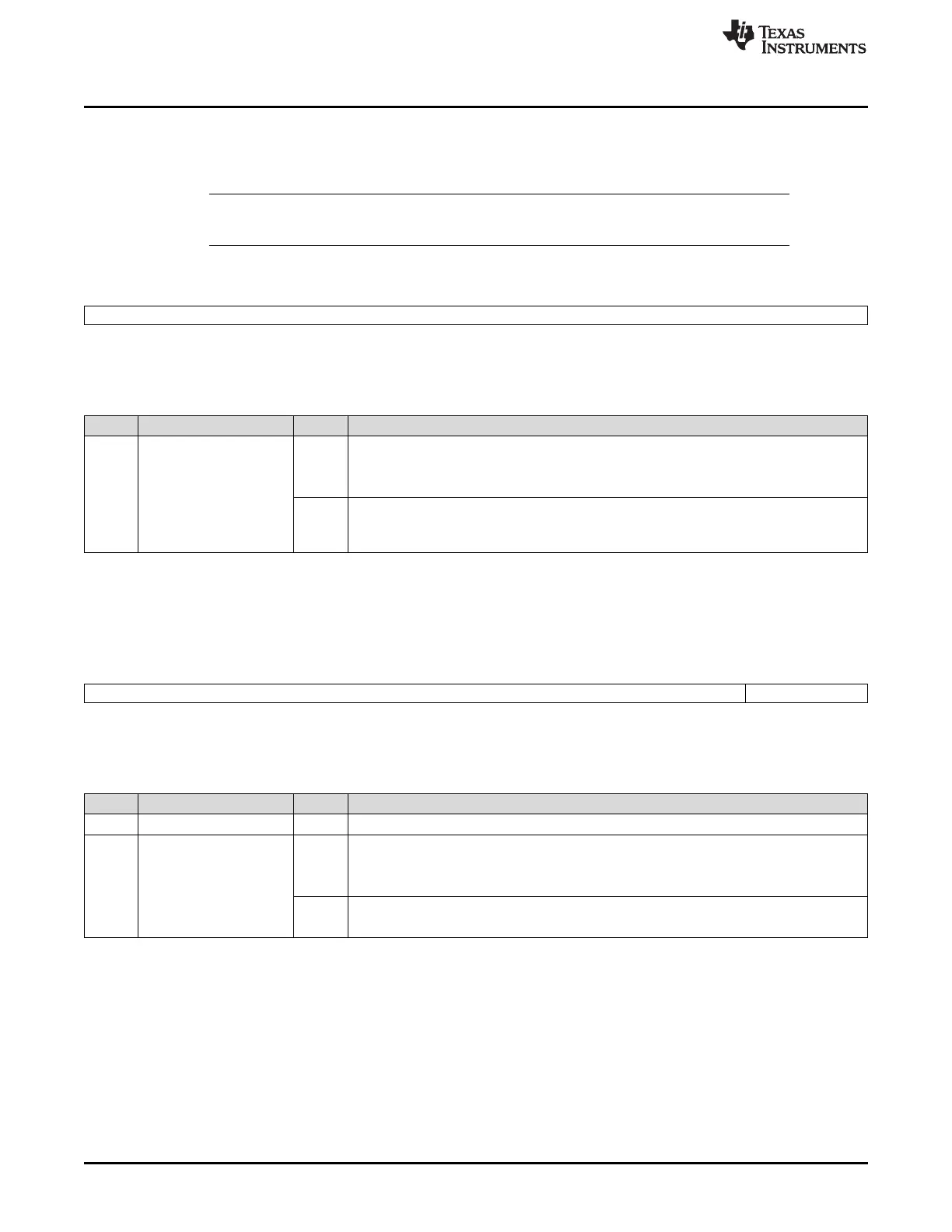
2.5.3.24 Peripheral Power-Down Clear Register 3 (PSPWRDWNCLR3)
There is one bit for each quadrant for PS24 to PS31. The protection scheme is described in
Section 2.5.3.17. This register is shown in Figure 2-95 and described in Table 2-109.
NOTE: Only those bits that have a slave at the corresponding bit position are implemented. Writes
to unimplemented bits have no effect and reads are 0.
Figure 2-95. Peripheral Power-Down Clear Register 3 (PSPWRDWNCLR) (offset = ACh)
31 0
PS[31-24]QUAD[3-0]PWRDWNCLR
R/WP-1
LEGEND: R/W = Read/Write; WP = Write in privileged mode only; -n = value after reset
Table 2-109. Peripheral Power-Down Clear Register 3 (PSPWRDWNCLR3) Field Descriptions
Bit Field Value Description
31-0 PS[31-24]QUAD[3-0]
PWRDWNCLR
Peripheral select quadrant clock power-down clear.
0 Read: The clock to the peripheral select quadrant is active.
Write: The bit is unchanged.
1 Read: The clock to the peripheral select quadrant is inactive.
Write: The corresponding bit in PSPWRDWNSET3 and PSPWRDWNCLR3 registers is
cleared to 0.
2.5.3.25 Debug Frame Powerdown Set Register (PDPWRDWNSET)
Figure 2-96. Debug Frame Powerdown Set Register (PDPWRDWNSET) (offset = C0h)
31 1 0
Reserved PDWRDWNSET
R-0 R/WP-1
LEGEND: R/W = Read/Write; R = Read only; WP = Write in privileged mode only; -n = value after reset
Table 2-110. Debug Frame Powerdown Set Register (PDPWRDWNSET) Field Descriptions
Bit Field Value Description
31-1 Reserved 0 Reads return 0. Writes have no effect.
0 PDWRDWNSET Debug Frame Powerdown Set Register.
0 Read: The clock to the debug frame is active.
Write: The bit is unchanged.
1 Read: The clock to the debug frame is inactive.
Write: Set the bit to 1.

 Loading...


