TC1796
Peripheral Units (Vol. 2 of 2)
Synchronous Serial Interface (SSC)
User’s Manual 20-28 V2.0, 2007-07
SSC, V2.1
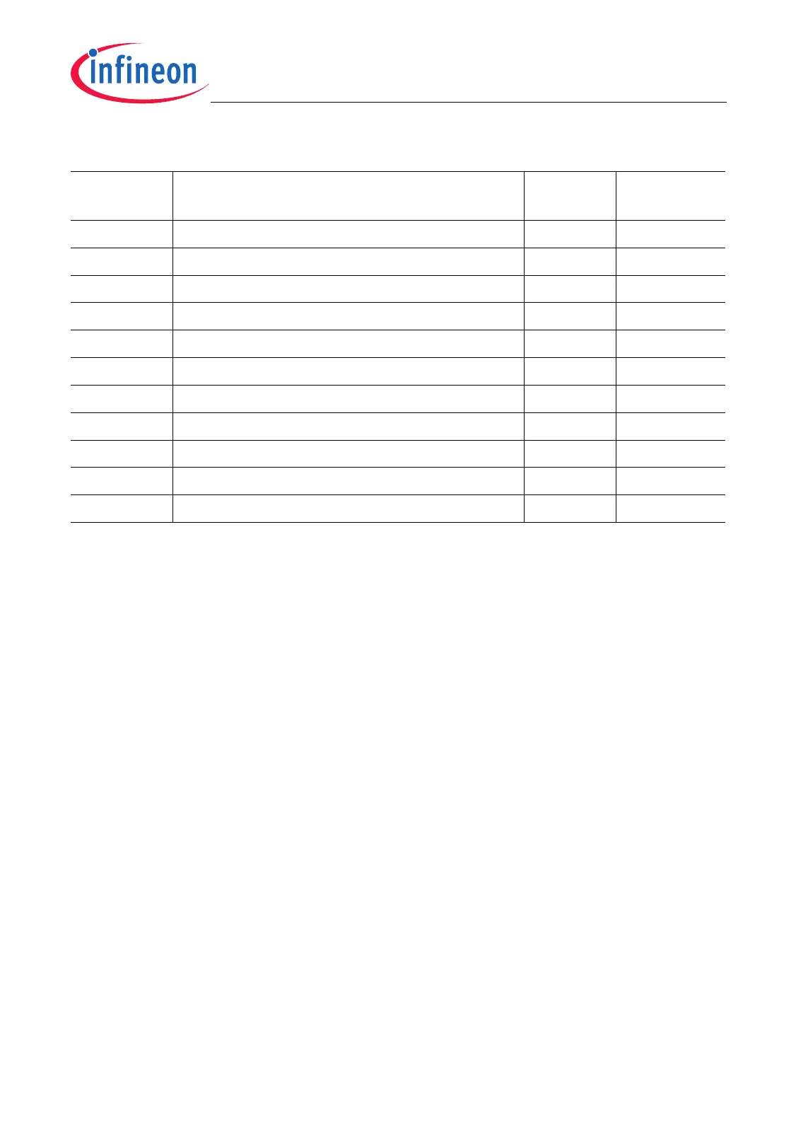
CON Control Register 10
H
Page 20-32
BR Baud Rate Timer Reload Register 14
H
Page 20-39
STAT Status Register 28
H
Page 20-34
EFM Error Flag Modification Register 2C
H
Page 20-35
SSOC Slave Select Output Control Register 18
H
Page 20-37
SSOTC Slave Select Output Timing Control Register 1C
H
Page 20-38
TB Transmit Buffer Register 20
H
Page 20-45
RB Receive Buffer Register 24
H
Page 20-45
RXFCON Receive FIFO Control Register 30
H
Page 20-40
TXFCON Transmit FIFO Control Register 34
H
Page 20-42
FSTAT FIFO Status Register 38
H
Page 20-44
1) The absolute register address is calculated as follows:
Module Base Address (Table 20-2) + Offset Address (shown in this column)
Table 20-3 Registers Overview - SSC Kernel Registers (cont’d)
Register
Short Name
Register Long Name Offset
Address
1)
Description
see

 Loading...