SYSCFG Registers
www.ti.com
228
SPRUH91D–March 2013–Revised September 2016
Submit Documentation Feedback
Copyright © 2013–2016, Texas Instruments Incorporated
System Configuration (SYSCFG) Module
10.5.12 Chip Signal Register (CHIPSIG)
The interrupts to the DSP can be generated by setting one of the two CHIPSIG[3-2] bits or an NMI
interrupt by setting the CHIPSIG[4] bit in the chip signal register (CHIPSIG). Writing a 1 to these bits sets
the interrupts, writing a 0 has no effect. Reads return the value of these bits and can also be used as
status bits. The CHIPSIG is shown in Figure 10-39 and described in Table 10-43.
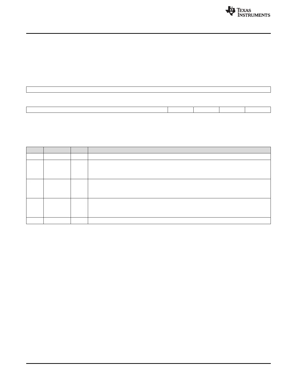
Figure 10-39. Chip Signal Register (CHIPSIG)
31 16
Reserved
R-0
15 5 4 3 2 1 0
Reserved CHIPSIG4 CHIPSIG3 CHIPSIG2 Reserved
R-0 R/W-0 R/W-0 R/W-0 R/W-0
LEGEND: R/W = Read/Write; R = Read only; -n = value after reset
Table 10-43. Chip Signal Register (CHIPSIG) Field Descriptions
Bit Field Value Description
31-5 Reserved 0 Reserved
4 CHIPSIG4 Asserts DSP NMI interrupt.
0 No effect
1 Asserts interrupt
3 CHIPSIG3 Asserts SYSCFG_CHIPINT3 interrupt.
0 No effect
1 Asserts interrupt
2 CHIPSIG2 Asserts SYSCFG_CHIPINT2 interrupt.
0 No effect
1 Asserts interrupt
1-0 Reserved 0 Reserved. Write the default value to all bits when modifying this register.