Bank
Row Col.
D1 D2 D3 D4
EMB_CLK
EMB_CS[0]
EMB_WE_DQM
EMB_BA
EMB_A
EMB_D
EMB_RAS
EMB_WE
EMB_CAS
WRT
ACTV
Architecture
www.ti.com
796
SPRUH91D–March 2013–Revised September 2016
Submit Documentation Feedback
Copyright © 2013–2016, Texas Instruments Incorporated
External Memory Interface B (EMIFB)
19.2.6.9 SDRAM Write Operations
When the EMIFB receives a write request to SDRAM , it performs one or more write-access cycles. A
write-access cycle begins with the issuing of the ACTV command to select the desired bank and row of
the SDRAM device. After the row has been opened, the EMIFB proceeds to issue a WRT command while
specifying the desired bank and column address. EMB_A[10] is held low during the WRT command to
avoid auto-precharging. The WRT command signals the SDRAM device to start writing a burst of data to
the specified address while the EMIFB issues NOP commands. The associated write data will be placed
on the data bus in the cycle concurrent with the WRT command and with subsequent burst continuation
NOP commands.
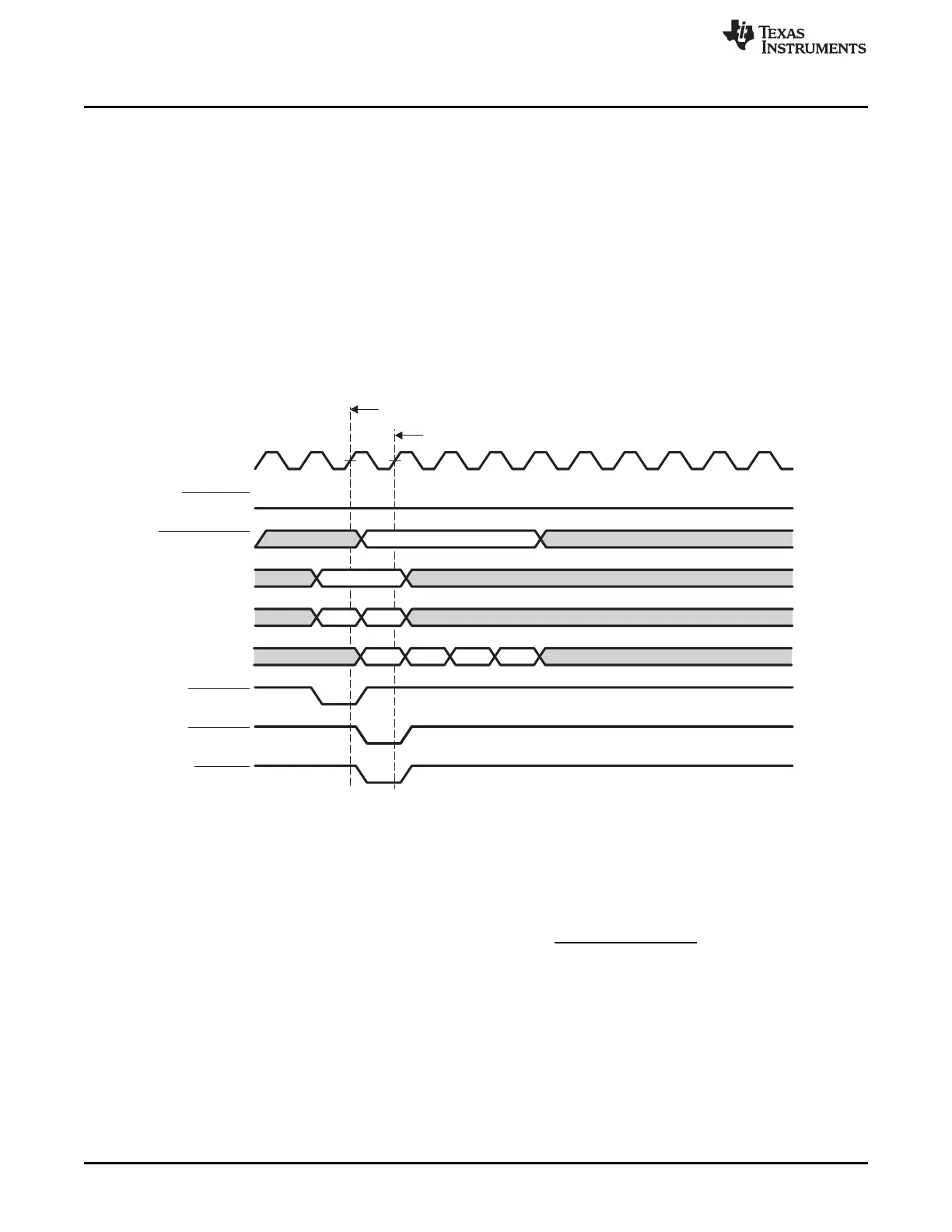
Figure 19-7 shows the signal waveforms for a basic SDRAM write operation in which a burst of data is
read from a single page. When the EMIFB SDRAM interface is configured to 32-bit by clearing the NM bit
of the SDRAM configuration register (SDCFG) to 0, a burst size of four is used. When configured to 16-bit
by setting NM to 1, a burst size of eight is used. Figure 19-7 shows a burst size of four.
Figure 19-7. Timing Waveform for Basic SDRAM Write Operation
The EMIFB will truncate a series of bursting data if the remaining addresses of the burst are not part of
the write request. The EMIFB can truncate the burst in three ways:
• By issuing another WRT to the same page
• By issuing a PRE command in order to prepare for accessing a different page of the same bank
• By issuing a BT command in order to prepare for accessing a page in a different bank
Several other pins are also active during a write access. The EMB_WE_DQM[3:0] pins are driven to select
which bytes of the data word will be written to the SDRAM device. They are also used to mask out entire
undesired data words during a burst access. The state of the other EMIFB pins during each command can
be found in Table 19-3.
EMIFB schedules its commands based on the timing information that is provided to it in the SDRAM timing
registers (SDTIM1 and SDTIM2). The values for the timing parameters in this register are chosen to
satisfy the timing requirements listed in the SDRAM datasheet. EMIFB uses this timing information to
avoid violating any timing constraints related to issuing commands. This is commonly accomplished by
inserting NOP commands during various cycles of an access. Refer to the register description of SDTIM1
and SDTIM2 for more details on the various timing parameters.

 Loading...


