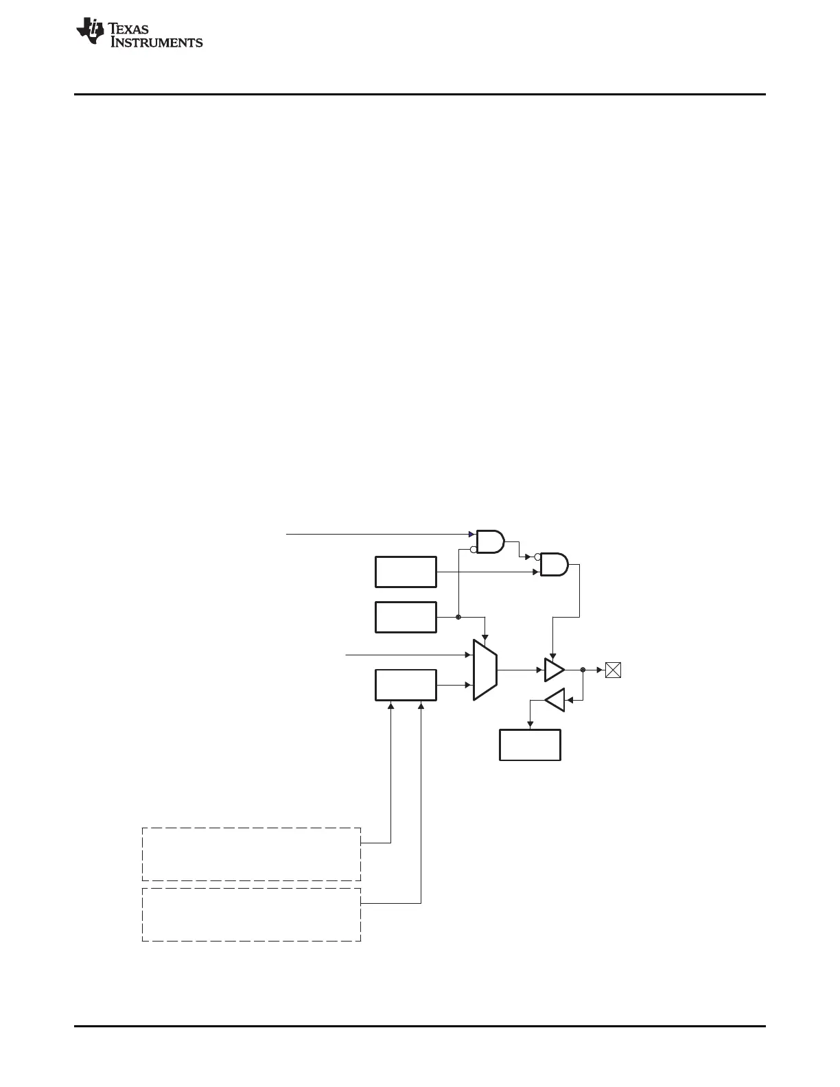
PDIR[n]
PFUNC[n]
0
1
PDOUT[n]
Disable path for
McASP serializer, set to 1 when:
a. Configured as transmitter
b. During inactive TDM slot
c. DISMODE is 3-state
McASP serializer
data out [n]
PDIN[n]
PDCLR[n]:
Writing 1 clears PDOUT[n] to 0
Writing 0 has no effect
Writing 1 sets PDOUT[n] to 1
PSET[n]:
Writing 0 has no effect
Clear if write 1
Set if write 1
AXR[n]
AHCLKR
ACLKR
AFSR
AHCLKX
ACLKX
AFSX
AMUTE
McASP I/O pins:
www.ti.com
1003
SPRUH91D–March 2013–Revised September 2016
Submit Documentation Feedback
Copyright © 2013–2016, Texas Instruments Incorporated
Multichannel Audio Serial Port (McASP)
Also, certain outputs require PDIR[n] = 1, such as clock pins used as clock outputs, serializer data pins
used to transmit, and AMUTE used as mute output.
Clock inputs and serializers configured to receive must have PDIR[n] = 0.
PFUNC and PDIR do not control the AMUTEIN device pin, it is usually tied to a device pin (see your
device-specific data manual). If used as a mute input, this pin needs to be configured as an input in the
appropriate peripheral.
Finally, there is an important advantage to having separate control of pin direction (by PDIR), and the
choice of internal versus external clocking (by CLKRM/CLKXM). Depending on the specific device and
usage, you might select an external clock (CLKRM = 0), while enabling the internal clock divider, and the
clock pin as an output in the PDIR register (PDIR[ACLKR] = 1). In this case, the bit clock is an output
(PDIR[ACLKR] = 1) and, therefore, routed to the ACLKR pin. However, because CLKRM = 0, the bit clock
is then routed back to the McASP module as an "external" clock source. This may result in less skew
between the clock inside the McASP and the clock in the external device, thus producing more balanced
setup and hold times for a particular system. As a result, this may allow a higher serial clock rate interface.
24.0.21.6.2 GPIO Pin Control
For GPIO operation, you must set the desired PFUNC[n] to 1 to indicate GPIO function. PDIR[n] must be
configured to the desired direction. PDOUT, PDSET, PDCLR control the output value on the pin. PDIN
always reflects the state at the pin, regardless of the PDIR and PFUNC setting.
Figure 24-21 and Figure 24-22 display the pin descriptions. The examples that follow (Example 24-1
through Example 24-4) show how the pins can be used as general-purpose input or output pins.
Figure 24-21. McASP I/O Pin Control Block Diagram
 Loading...


