1, 2, 4, 8 BPP12, 16 BPP
Palette
Input
FIFO
STN
(passive)
TFT
(active)
1, 2, 4, 8 BPP 16 BPP
Gray-scaler/
serializer
Output FIFO
Palette
Output FIFO
Output pins
Data source
(frame buffers)
Gray-scaler/
serializer
Architecture
www.ti.com
940
SPRUH91D–March 2013–Revised September 2016
Submit Documentation Feedback
Copyright © 2013–2016, Texas Instruments Incorporated
Liquid Crystal Display Controller (LCDC)
23.2.5.1 Logical Data Path
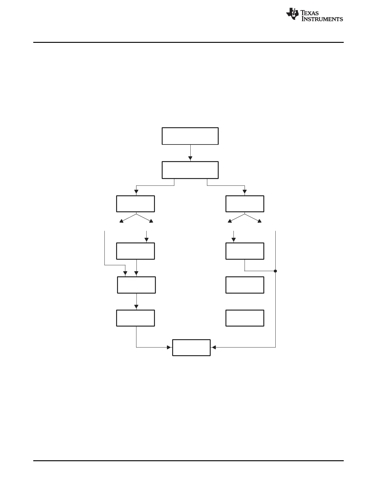
The block diagram of the Raster Controller is shown in Figure 23-1. Figure 23-3 illustrates its logical data
path for various operation modes (passive (STN) versus active (TFT), various BPP size).
Figure 23-3 shows that:
• The gray-scaler/serializer and output FIFO blocks are bypassed in active (TFT) modes.
• The palette is bypassed in both 12- and 16-BPP modes.
Figure 23-3. Logical Data Path for Raster Controller
In summary:
• The display image is stored in frame buffers.
• The built-in DMA engine constantly transfers the data stored in the frame buffers to the Input FIFO.
• The Raster Controller relays data to the external pins according to the specified format.
The remainder of this section describes the functioning blocks in Figure 23-3, including frame buffers,
palette, and gray-scaler/serializer. Their operation and programming techniques are covered in detail. The
output format is also described in Section 23.2.5.5.



 To Next Page