Registers
www.ti.com
928
SPRUH91D–March 2013–Revised September 2016
Submit Documentation Feedback
Copyright © 2013–2016, Texas Instruments Incorporated
Inter-Integrated Circuit (I2C) Module
22.3.19 I2C Pin Data Out Register (ICPDOUT)
The I2C pin data out register (ICPDOUT) has one bit for each of the GPIO pins. This bit holds a value for
data out at all times, and may be read back at all times. The value held by this register is not affected by
writing to the PDIR and PFUNC bits. However, the data value in this register is driven out onto the GPIO
pin only if the PFUNC0 bit in ICPFUNC is set to 1 (I2Cx_SDA and I2Cx_SCL function as GPIO) and also
the corresponding bit in ICPDIR is set to 1 (output).
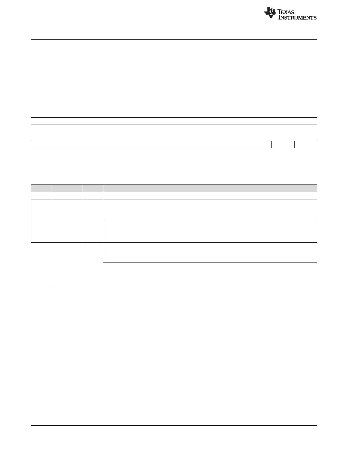
ICPDOUT is shown in Figure 22-33 and described in Table 22-26.
Figure 22-33. I2C Pin Data Out Register (ICPDOUT)
31 16
Reserved
R-0
15 2 1 0
Reserved PDOUT1 PDOUT0
R-0 R/W-0 R/W-0
LEGEND: R/W = Read/Write; R = Read only; -n = value after reset
Table 22-26. I2C Pin Data Out Register (ICPDOUT) Field Descriptions
Bit Field Value Description
31-2 Reserved 0 These reserved bit locations are always read as zeros. A value written to this field has no effect.
1 PDOUT1 Controls the level driven on the I2Cx_SDA pin when configured as GPIO output. Note: If I2Cx_SDA is
connected to an open-drain buffer at the chip level, the I2C cannot drive I2Cx_SDA to high.
During reads: Reads return register values, not GPIO pin levels.
During writes:
0 I2Cx_SDA pin is driven low.
1 I2Cx_SDA pin is driven high.
0 PDOUT0 Controls the level driven on the I2Cx_SCL pin when configured as GPIO output. Note: If I2Cx_SCL is
connected to an open-drain buffer at the chip level, the I2C cannot drive I2Cx_SCL to high.
During reads: Reads return register values, not GPIO pin levels.
During writes:
0 I2Cx_SCL pin is driven low.
1 I2Cx_SCL pin is driven high.

 Loading...


