www.ti.com
Registers
841
SPRUH91D–March 2013–Revised September 2016
Submit Documentation Feedback
Copyright © 2013–2016, Texas Instruments Incorporated
General-Purpose Input/Output (GPIO)
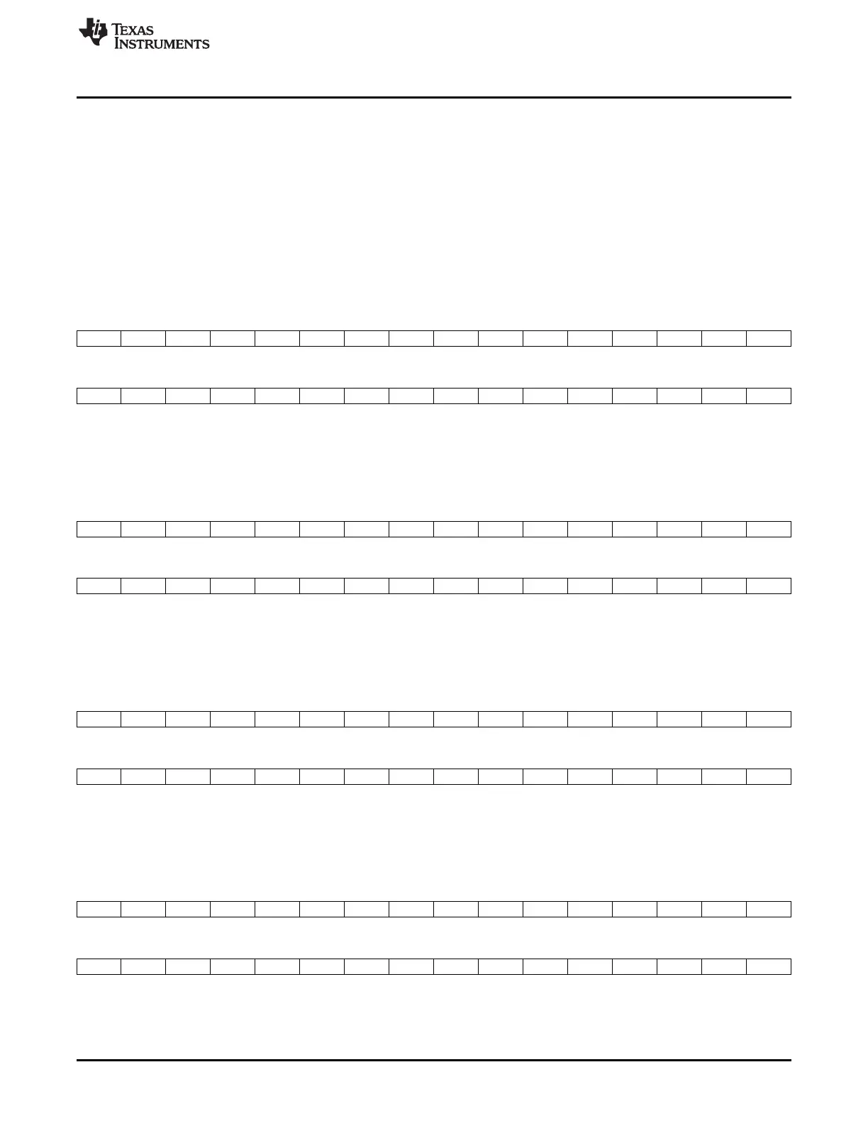
20.3.5 GPIO Set Data Registers (SET_DATAn)
The GPIO set data register (SET_DATAn) controls driving high of the corresponding GPIO pin j in GPIO
bank k, if the pin is configured as an output (DIRn = 0). Writes do not affect pins not configured as GPIO
outputs. Writing a 1 to a specific bit in SET_DATAn sets the corresponding GPIO pin j in GPIO bank k. A
read of the BkPj bit returns the output drive state of the corresponding pin GPIOk[j]. The GPIO set data
register (SET_DATA01) is shown in Figure 20-14, SET_DATA23 is shown in Figure 20-15, SET_DATA45
is shown in Figure 20-16, SET_DATA67 is shown in Figure 20-17, SET_DATA8 is shown in Figure 20-18,
and described in Table 20-7. See Table 20-1 to determine the SET_DATAn bit associated with each GPIO
bank and pin number.
Figure 20-14. GPIO Banks 0 and 1 Set Data Register (SET_DATA01)
31 30 29 28 27 26 25 24 23 22 21 20 19 18 17 16
GP1P15 GP1P14 GP1P13 GP1P12 GP1P11 GP1P10 GP1P9 GP1P8 GP1P7 GP1P6 GP1P5 GP1P4 GP1P3 GP1P2 GP1P1 GP1P0
R/W-0
15 14 13 12 11 10 9 8 7 6 5 4 3 2 1 0
GP0P15 GP0P14 GP0P13 GP0P12 GP0P11 GP0P10 GP0P9 GP0P8 GP0P7 GP0P6 GP0P5 GP0P4 GP0P3 GP0P2 GP0P1 GP0P0
R/W-0
LEGEND: R/W = Read/Write; -n = value after reset
Figure 20-15. GPIO Banks 2 and 3 Set Data Register (SET_DATA23)
31 30 29 28 27 26 25 24 23 22 21 20 19 18 17 16
GP3P15 GP3P14 GP3P13 GP3P12 GP3P11 GP3P10 GP3P9 GP3P8 GP3P7 GP3P6 GP3P5 GP3P4 GP3P3 GP3P2 GP3P1 GP3P0
R/W-0
15 14 13 12 11 10 9 8 7 6 5 4 3 2 1 0
GP2P15 GP2P14 GP2P13 GP2P12 GP2P11 GP2P10 GP2P9 GP2P8 GP2P7 GP2P6 GP2P5 GP2P4 GP2P3 GP2P2 GP2P1 GP2P0
R/W-0
LEGEND: R/W = Read/Write; -n = value after reset
Figure 20-16. GPIO Banks 4 and 5 Set Data Register (SET_DATA45)
31 30 29 28 27 26 25 24 23 22 21 20 19 18 17 16
GP5P15 GP5P14 GP5P13 GP5P12 GP5P11 GP5P10 GP5P9 GP5P8 GP5P7 GP5P6 GP5P5 GP5P4 GP5P3 GP5P2 GP5P1 GP5P0
R/W-0
15 14 13 12 11 10 9 8 7 6 5 4 3 2 1 0
GP4P15 GP4P14 GP4P13 GP4P12 GP4P11 GP4P10 GP4P9 GP4P8 GP4P7 GP4P6 GP4P5 GP4P4 GP4P3 GP4P2 GP4P1 GP4P0
R/W-0
LEGEND: R/W = Read/Write; -n = value after reset
Figure 20-17. GPIO Banks 6 and 7 Set Data Register (SET_DATA67)
31 30 29 28 27 26 25 24 23 22 21 20 19 18 17 16
GP7P15 GP7P14 GP7P13 GP7P12 GP7P11 GP7P10 GP7P9 GP7P8 GP7P7 GP7P6 GP7P5 GP7P4 GP7P3 GP7P2 GP7P1 GP7P0
R/W-0
15 14 13 12 11 10 9 8 7 6 5 4 3 2 1 0
GP6P15 GP6P14 GP6P13 GP6P12 GP6P11 GP6P10 GP6P9 GP6P8 GP6P7 GP6P6 GP6P5 GP6P4 GP6P3 GP6P2 GP6P1 GP6P0
R/W-0
LEGEND: R/W = Read/Write; -n = value after reset

 Loading...


