Registers
www.ti.com
950
SPRUH91D–March 2013–Revised September 2016
Submit Documentation Feedback
Copyright © 2013–2016, Texas Instruments Incorporated
Liquid Crystal Display Controller (LCDC)
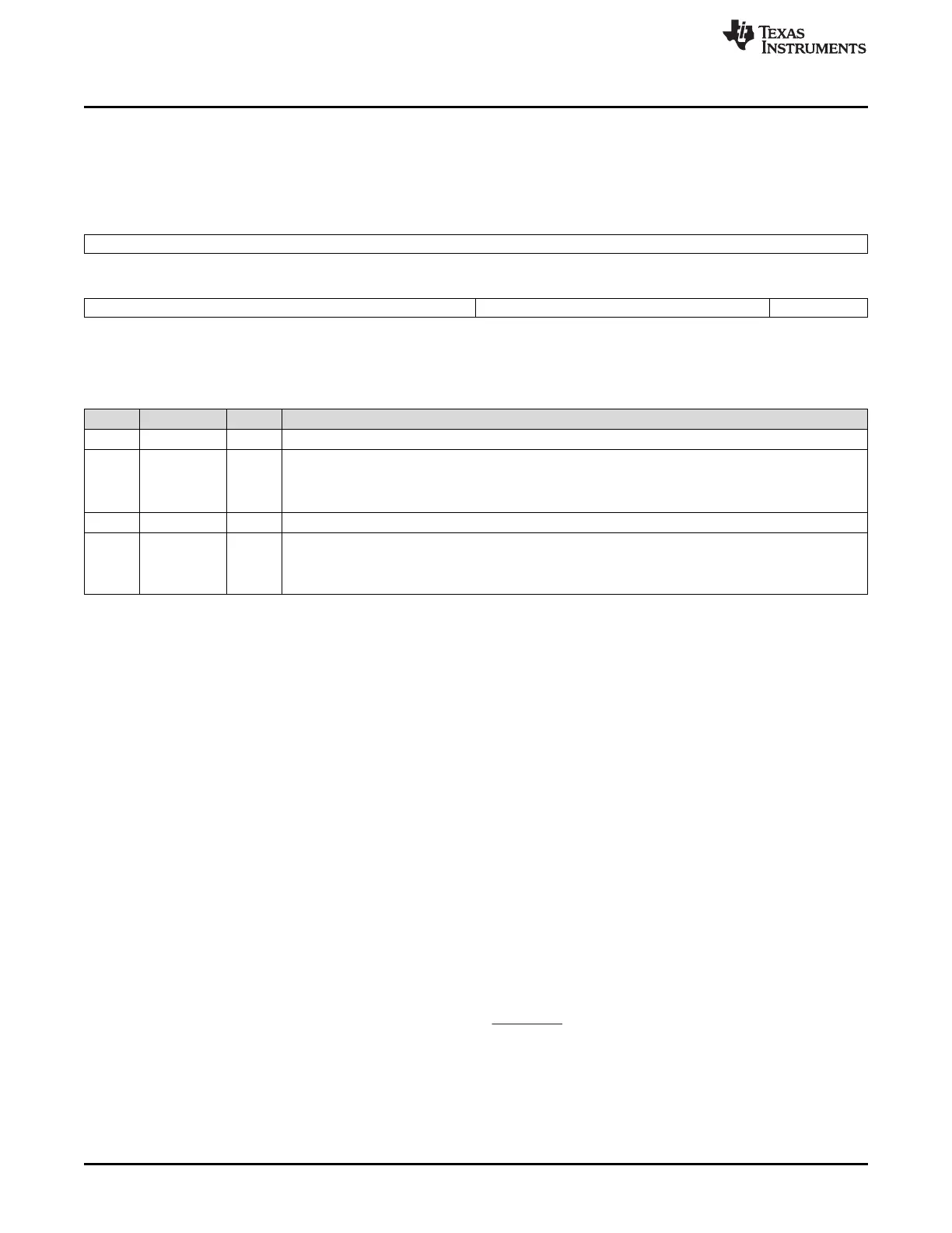
23.3.2 LCD Control Register (LCD_CTRL)
The LCD control register (LCD_CTRL) contains the fundamental mode select bit for the LCD controller.
The LCD_CTRL is shown in Figure 23-16 and described in Table 23-11.
Figure 23-16. LCD Control Register (LCD_CTRL)
31 16
Reserved
R-0
15 8 7 1 0
CLKDIV Reserved MODESEL
R/W-0 R-0 R/W-0
LEGEND: R/W = Read/Write; R = Read only; -n = value after reset
Table 23-11. LCD Control Register (LCD_CTRL) Field Descriptions
Bit Field Value Description
31-16 Reserved 0 Reserved
15-8 CLKDIV 0-FFh Clock Divisor. Value (from 0 to 255) is used to specify the frequency of the pixel clock (in Raster mode)
or MCLK (in LIDD mode) based on the LCD_CLK frequency. Pixel clock frequency can range from
LCD_CLK/2 to LCD_CLK/255 (CLKDIV = 0 or CLKDIV = 1 are not valid). MCLK can vary from
LCD_CLK to LCD_CLK/255 (CLKDIV = 0 or CLKDIV = 1 sets MCLK = LCD_CLK).
7-1 Reserved 0 Reserved
0 MODESEL LCD Mode Select
0 LCD Controller in LIDD mode
1 LCD Controller in Raster mode
The 8-bit clock divider (CLKDIV) field is used to select the frequency of the pixel clock. CLKDIV can
generate a range of pixel clock frequencies from LCD_CLK/2 to LCD_CLK/255. The pixel clock frequency
must be adjusted to meet the required screen refresh rate.
The refresh rate depends on:
• The number of pixels for the target display.
• Whether monochrome or color mode is selected.
• The number of pixel clock delays programmed at the beginning and end of each line.
• The number of line clocks inserted at the beginning and end of each frame.
• The width of the frame clock (LCD_VSYNC) signal in active mode or VSW line clocks inserted in
passive mode.
• The width of the line clock (LCD_HSYNC) signal.
All of these factors alter the time duration from one frame transmission to the next. Different display
manufacturers require different frame refresh rates, depending on the physical characteristics of the
display. CLKDIV is used to alter the pixel clock frequency in order to meet these requirements. Pixel clock
is used to synchronously signal the device to drive data to the LCD data pins, and to signal the output
FIFO to latch the data from the pins. The frequency of the pixel clock for a set CLKDIV value or the
required CLKDIV value to yield a target pixel clock frequency can be calculated using the following
equation: