Registers
www.ti.com
774
SPRUH91D–March 2013–Revised September 2016
Submit Documentation Feedback
Copyright © 2013–2016, Texas Instruments Incorporated
External Memory Interface A (EMIFA)
18.4.13 NAND Flash Status Register (NANDFSR)
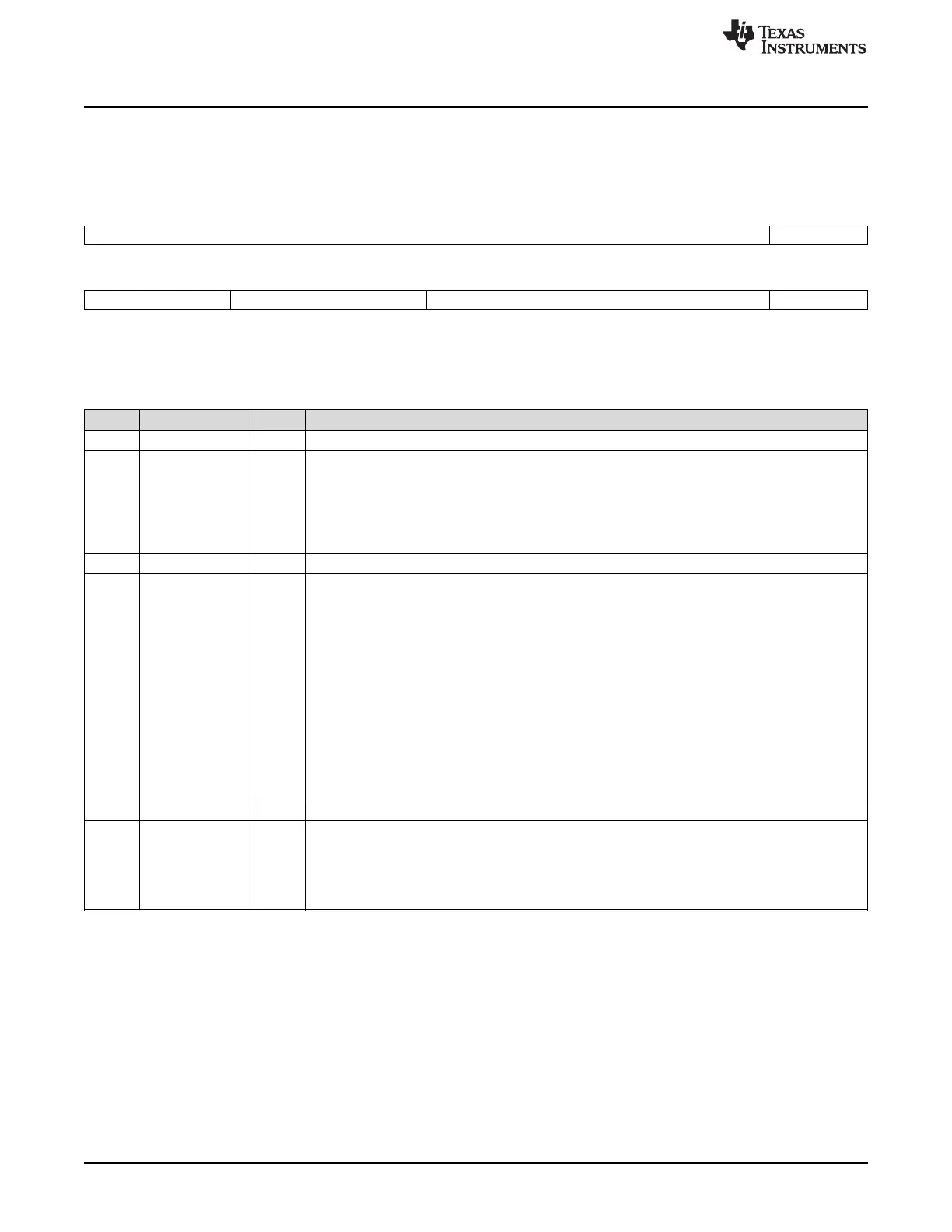
The NAND Flash status register (NANDFSR) is shown in Figure 18-43 and described in Table 18-61.
Figure 18-43. NAND Flash Status Register (NANDFSR)
31 18 17 16
Reserved ECC_ERRNUM
R-0 R-0
15 12 11 8 7 2 1 0
Reserved ECC_STATE Reserved WAITST[n]
R-0 R-0 R-0 R-0
LEGEND: R = Read only; -n = value after reset
Table 18-61. NAND Flash Status Register (NANDFSR) Field Descriptions
Bit Field Value Description
31-18 Reserved 0 Reserved
17-16 ECC_ERRNUM 0-3h Number of Errors found after the 4-Bit ECC Error Address and Error Value Calculation.
0 1 error found.
1h 2 errors found.
2h 3 errors found.
3h 4 errors found.
15-12 Reserved 0 Reserved.
11-8 ECC_STATE 0-Fh ECC correction state while performing 4-bit ECC Address and Error Value Calculation
0 No errors detected
1h Errors cannot be corrected (5 or more)
2h Error correction complete(errors on bit 8 or 9).
3h Error correction complete(error exists).
4h Reserved.
5h Calculating number of errors
6h-7h Preparing for error search
8h Searching for errors
9h-Bh Reserved.
Ch-Fh Calculating error value
7-2 Reserved 0 Reserved.
1-0 WAITST[n] Status of the EMA_WAIT[n] input pins. Not all devices support both EMA_WAIT[1] and
EMA_WAIT[0], see the device-specific data manual to determine support on each device. The WPn
bit in the asynchronous wait cycle configuration register (AWCC) has no effect on WAITST.
0 EMA_WAIT[n] pin is low.
1 EMA_WAIT[n] pin is high.



 To Next Page