www.ti.com
Registers
565
SPRUH91D–March 2013–Revised September 2016
Submit Documentation Feedback
Copyright © 2013–2016, Texas Instruments Incorporated
Enhanced Direct Memory Access (EDMA3) Controller
16.4.3.6.16 Destination FIFO Destination Address Register n (DFDSTn)
The destination FIFO destination address register n (DFDSTn) is shown in Figure 16-106 and described in
Table 16-86.
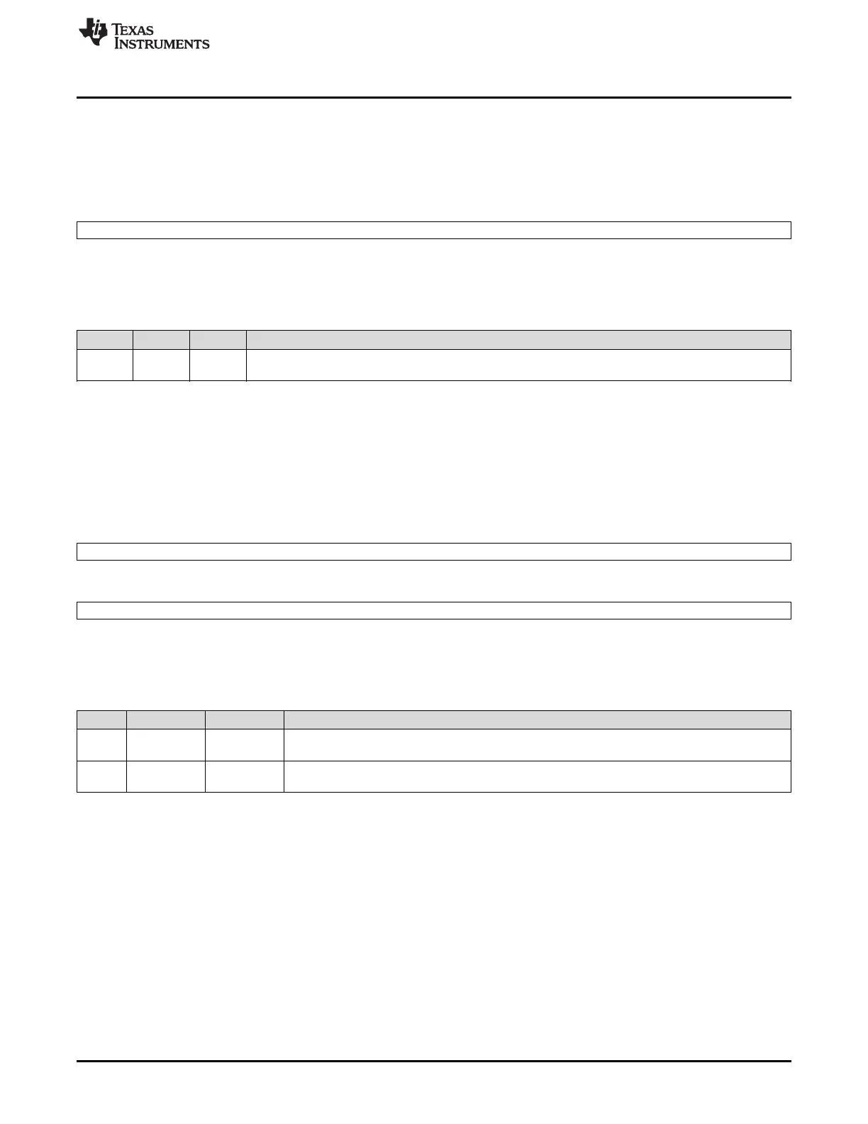
Figure 16-106. Destination FIFO Destination Address Register n (DFDSTn)
31 0
DADDR
R-0
LEGEND: R = Read only; -n = value after reset
Table 16-86. Destination FIFO Destination Address Register n (DFDSTn) Field Descriptions
Bit Field Value Description
31-0 DADDR 0 Destination address for the destination FIFO register set. When a transfer request (TR) is complete, the
final value should be the address of the last write command issued.
16.4.3.6.17 Destination FIFO B-Index Register n (DFBIDXn)
The destination FIFO B-index register n (DFBIDXn) is shown in Figure 16-107 and described in
Table 16-87.
Figure 16-107. Destination FIFO B-Index Register n (DFBIDXn)
31 16
DSTBIDX
R-0
15 0
SRCBIDX
R-0
LEGEND: R = Read only; -n = value after reset
Table 16-87. Destination FIFO B-Index Register n (DFBIDXn) Field Descriptions
Bit Field Value Description
31-16 DSTBIDX 0-FFFFh B-Index offset between destination arrays. Represents the offset in bytes between the starting
address of each destination.
15-0 SRCBIDX 0 B-Index offset between source arrays. Represents the offset in bytes between the starting address
of each source array. Always Read as 0.