www.ti.com
Registers
855
SPRUH91D–March 2013–Revised September 2016
Submit Documentation Feedback
Copyright © 2013–2016, Texas Instruments Incorporated
General-Purpose Input/Output (GPIO)
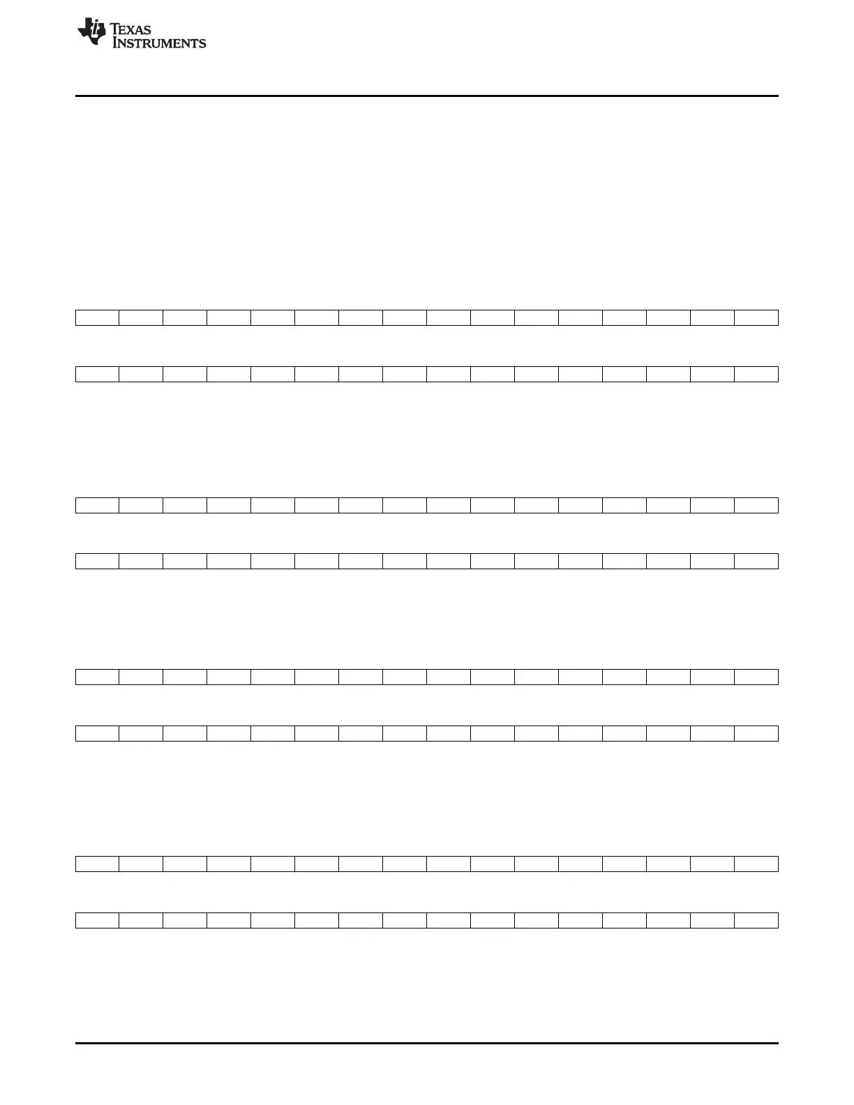
20.3.12 GPIO Interrupt Status Registers (INTSTATn)
The status of GPIO interrupt events can be monitored by reading the GPIO interrupt status register
(INTSTATn). In the associated bit position, pending GPIO interrupts are indicated with a logic 1 and GPIO
interrupts that are not pending are indicated with a logic 0. The GPIO interrupt status register
(INTSTAT01) is shown in Figure 20-49, INTSTAT23 is shown in Figure 20-50, INTSTAT45 is shown in
Figure 20-51, INTSTAT67 is shown in Figure 20-52, INTSTAT8 is shown in Figure 20-53, and described in
Table 20-14. See Table 20-1 to determine the INTSTATn bit associated with each GPIO bank and pin
number.
Figure 20-49. GPIO Banks 0 and 1 Interrupt Status Register (INTSTAT01)
31 30 29 28 27 26 25 24 23 22 21 20 19 18 17 16
GP1P15 GP1P14 GP1P13 GP1P12 GP1P11 GP1P10 GP1P9 GP1P8 GP1P7 GP1P6 GP1P5 GP1P4 GP1P3 GP1P2 GP1P1 GP1P0
R/W1C-0
15 14 13 12 11 10 9 8 7 6 5 4 3 2 1 0
GP0P15 GP0P14 GP0P13 GP0P12 GP0P11 GP0P10 GP0P9 GP0P8 GP0P7 GP0P6 GP0P5 GP0P4 GP0P3 GP0P2 GP0P1 GP0P0
R/W1C-0
LEGEND: R/W = Read/Write; W1C = Write 1 to clear bit (writing 0 has no effect); -n = value after reset
Figure 20-50. GPIO Banks 2 and 3 Interrupt Status Register (INTSTAT23)
31 30 29 28 27 26 25 24 23 22 21 20 19 18 17 16
GP3P15 GP3P14 GP3P13 GP3P12 GP3P11 GP3P10 GP3P9 GP3P8 GP3P7 GP3P6 GP3P5 GP3P4 GP3P3 GP3P2 GP3P1 GP3P0
R/W1C-0
15 14 13 12 11 10 9 8 7 6 5 4 3 2 1 0
GP2P15 GP2P14 GP2P13 GP2P12 GP2P11 GP2P10 GP2P9 GP2P8 GP2P7 GP2P6 GP2P5 GP2P4 GP2P3 GP2P2 GP2P1 GP2P0
R/W1C-0
LEGEND: R/W = Read/Write; W1C = Write 1 to clear bit (writing 0 has no effect); -n = value after reset
Figure 20-51. GPIO Banks 4 and 5 Interrupt Status Register (INTSTAT45)
31 30 29 28 27 26 25 24 23 22 21 20 19 18 17 16
GP5P15 GP5P14 GP5P13 GP5P12 GP5P11 GP5P10 GP5P9 GP5P8 GP5P7 GP5P6 GP5P5 GP5P4 GP5P3 GP5P2 GP5P1 GP5P0
R/W1C-0
15 14 13 12 11 10 9 8 7 6 5 4 3 2 1 0
GP4P15 GP4P14 GP4P13 GP4P12 GP4P11 GP4P10 GP4P9 GP4P8 GP4P7 GP4P6 GP4P5 GP4P4 GP4P3 GP4P2 GP4P1 GP4P0
R/W1C-0
LEGEND: R/W = Read/Write; W1C = Write 1 to clear bit (writing 0 has no effect); -n = value after reset
Figure 20-52. GPIO Banks 6 and 7 Interrupt Status Register (INTSTAT67)
31 30 29 28 27 26 25 24 23 22 21 20 19 18 17 16
GP7P15 GP7P14 GP7P13 GP7P12 GP7P11 GP7P10 GP7P9 GP7P8 GP7P7 GP7P6 GP7P5 GP7P4 GP7P3 GP7P2 GP7P1 GP7P0
R/W1C-0
15 14 13 12 11 10 9 8 7 6 5 4 3 2 1 0
GP6P15 GP6P14 GP6P13 GP6P12 GP6P11 GP6P10 GP6P9 GP6P8 GP6P7 GP6P6 GP6P5 GP6P4 GP6P3 GP6P2 GP6P1 GP6P0
R/W1C-0
LEGEND: R/W = Read/Write; W1C = Write 1 to clear bit (writing 0 has no effect); -n = value after reset