Registers
www.ti.com
844
SPRUH91D–March 2013–Revised September 2016
Submit Documentation Feedback
Copyright © 2013–2016, Texas Instruments Incorporated
General-Purpose Input/Output (GPIO)
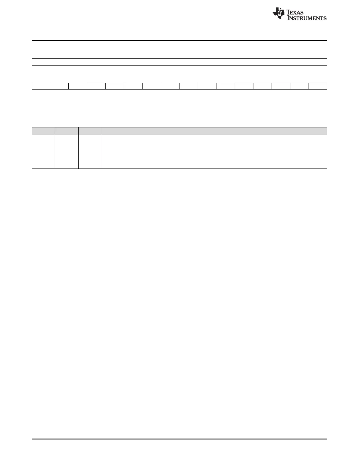
Figure 20-23. GPIO Bank 8 Clear Data Register (CLR_DATA8)
31 16
Reserved
R/W-0
15 14 13 12 11 10 9 8 7 6 5 4 3 2 1 0
GP8P15 GP8P14 GP8P13 GP8P12 GP8P11 GP8P10 GP8P9 GP8P8 GP8P7 GP8P6 GP8P5 GP8P4 GP8P3 GP8P2 GP8P1 GP8P0
R/W-0
LEGEND: R/W = Read/Write; -n = value after reset
Table 20-8. GPIO Clear Data Register (CLR_DATAn) Field Descriptions
Bit Field Value Description
31-0 GPkPj Clear the output drive state of GPk[j] to logic low. The GPkPj bit is used to drive the output low on pin j in
GPIO bankk. The GPkPj bit is ignored when GPk[j] is configured as an input. Reading the GPkPj bit
returns the output drive state of GPk[j].
0 No effect.
1 GPk[j] is set to output logic low.

 Loading...


