www.ti.com
Architecture
797
SPRUH91D–March 2013–Revised September 2016
Submit Documentation Feedback
Copyright © 2013–2016, Texas Instruments Incorporated
External Memory Interface B (EMIFB)
19.2.6.10 Mapping from Logical Address to EMIFB Pins
When the EMIFB receives an SDRAM access request, it must convert the address of the access into the
appropriate signals to send to the SDRAM device. The details of an example address mapping are shown
in Table 19-14 for 32-bit operation and in Table 19-15 for 16-bit operation. (In both the examples, a 13-bit
row address is used to calculate the maximum reach. See your device-specific data manual to know the
possible values of IBANK and PAGESIZE for EMIFB). Using the settings of the IBANK and PAGESIZE
fields of the SDRAM configuration register (SDCFG), the EMIFB determines which bits of the logical
address will be mapped to the SDRAM row, column, and bank addresses.
As the logical address is incremented by one word (32-bit operation) or one halfword (16-bit operation),
the column address is likewise incremented by one until a page boundary is reached. When the logical
address increments across a page boundary, the EMIFB moves into the same page in the next bank of
the attached device by incrementing the bank address EMB_BA and resetting the column address. The
page in the previous bank is left open until it is necessary to close it. This method of traversal through the
SDRAM banks helps maximize the number of open banks inside of the SDRAM and results in an efficient
use of the device. There is no limitation on the number of banks than can be open at one time, but only
one page within a bank can be open at a time. To use such an addressing scheme, clear the internal bank
position (IBANK_POS) bit in SDCFG to 0. This addressing scheme is used when EMIFB memory
controller is configured to interface with SDR SDRAM.
The EMIFB uses the EMB_WE_DQM pins during a WRT command to mask out selected bytes or entire
words. The EMB_WE_DQM pins are always low during a READ command.
When using mobile SDRAM, set IBANK_POS = 1, and this uses an addressing scheme as described in
Table 19-16. See device data manual to know possible values of ROWSIZE, IBANK, and PAGESIZE for
EMIFB configured to interface with mobile SDRAM device.
When the IBANK_POS bit is set to 1, the PAGESIZE, ROWSIZE, and IBANK fields control the mapping of
the logical source address of the memory controller to the column, row, and bank address bits of the
SDRAM device. Table 19-16 shows which source address bits map to the SDRAM column, row, and bank
address bits for all combinations of PAGESIZE, ROWSIZE, and IBANK.
When the IBANK_POS bit is set to 1, the effect of the address-mapping scheme is that as the source
address increments across an SDRAM page boundary, the memory controller proceeds to the next page
in the same bank. This movement along the same bank continues until all the pages have been accessed
in the same bank. The memory controller then proceeds to the next bank in the device. Since, in this
address mapping scheme, the memory controller can keep only one bank open, this scheme is lower in
performance than the case when IBANK_POS is cleared to 0. Therefore, this case is only recommended
to be used with Partial Array Self-refresh for mobile SDR SDRAM where performance may be traded-off
for power savings.
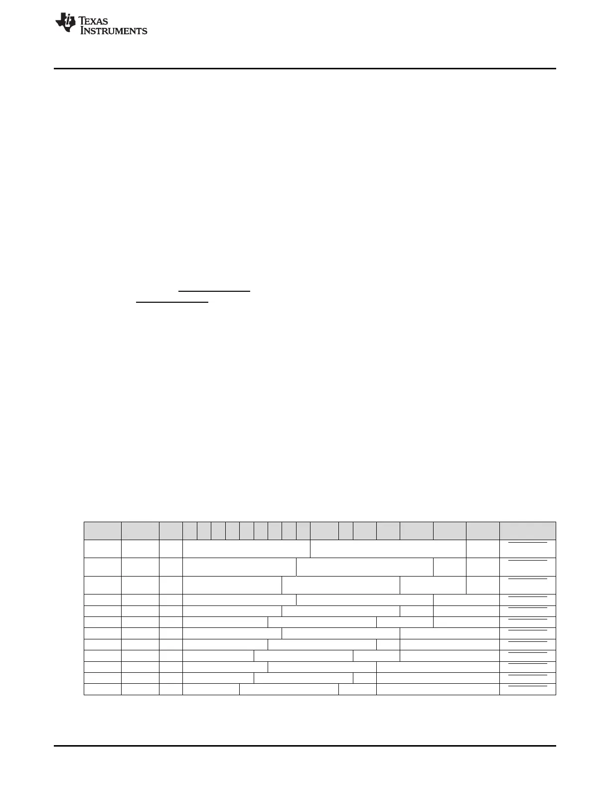
Table 19-14. Example Mapping from Logical Address to EMIFB Pins for 32-bit SDRAM
REACH
(MB) IBANK
PAGE
SIZE 31 30 29 28 27 26 25 24 23 22:15 14 13 12 11 10 9:2 1:0
8 0 0 - Row Address Column
Address
WE_DQM[3:0]
16 1 0 - Row Address BA[0] Column
Address
WE_DQM[3:0]
32 2 0 - Row Address BA[1:0] Column
Address
WE_DQM[3:0]
16 0 1 - Row Address Column Address WE_DQM[3:0]
32 1 1 - Row Address BA[0] Column Address WE_DQM[3:0]
64 2 1 - Row Address BA[1:0] Column Address WE_DQM[3:0]
32 0 2 - Row Address Column Address WE_DQM[3:0]
64 1 2 - Row Address BA[0] Column Address WE_DQM[3:0]
128 2 2 - Row Address BA[1:0] Column Address WE_DQM[3:0]
64 0 3 - Row Address Column Address WE_DQM[3:0]
128 1 3 - Row Address BA[0] Column Address WE_DQM[3:0]
256 2 3 - Row Address BA[1:0] Column Address WE_DQM[3:0]

 Loading...


