Setup
Strobe
Hold
t
RC
(m)
t
RP
(m)
t
REA
(m)
t
CEA
(m)
t
SU
t
RHZ
(m)
t
H
t
CHZ
(m)
EMA_CS[n]
ALE_EM_A[1]
CLE_EM_A[2]
EMA_OE
EMA_D[7:0]
t
CLR
(m)
TA w max
ǒ
t
CHZ
(m)
t
cyc
,
t
RHZ
(m) * (R_HOLD ) 1)t
cyc
t
cyc
Ǔ
* 1
R_SETUP ) R_STROBE ) R_HOLD w
t
RC
(m)
t
cyc
* 3
R_HOLD w
ǒ
t
H
* t
CHZ
(m)
Ǔ
t
cyc
* 1
R_SETUP + R_STROBE ≥
t
CEA
(m) t
SU
t
cyc
- 2
( )
+
R_STROBE w max
ǒ
ǒ
t
REA
(m) ) t
SU
Ǔ
t
cyc
,
t
RP
(m)
t
cyc
Ǔ
* 1
www.ti.com
Example Configuration
751
SPRUH91D–March 2013–Revised September 2016
Submit Documentation Feedback
Copyright © 2013–2016, Texas Instruments Incorporated
External Memory Interface A (EMIFA)
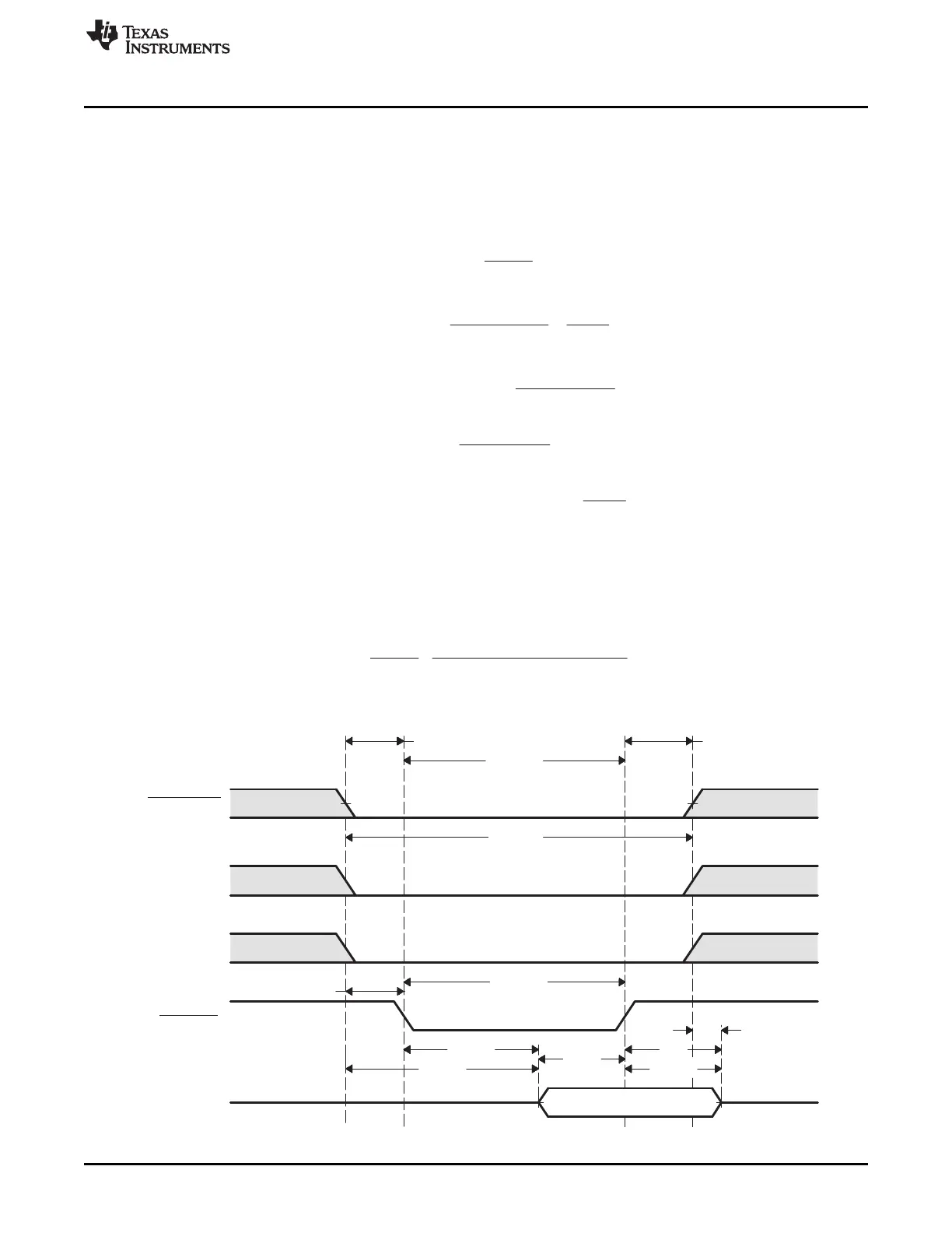
From Figure 18-27, the following equations may be derived. t
cyc
is the period at which the EMIFA operates.
The R_SETUP, R_STROBE, and R_HOLD fields are programmed in terms of EMIFA cycles where as the
data sheet specifications are typically given is nano seconds. This is explains the presence of t
cyc
in the
denominator of the following equations. A minus 1 is included in the equations because each field in
CEnCFG is programmed in terms of EMIFA clock cycles, minus 1 cycle. For example, R_SETUP is equal
to R_SETUP width in EMIFA clock cycles minus 1 cycle.
The EMIFA offers an additional parameter, TA, that defines the turnaround time between read and write
cycles. This parameter protects against the situation when the output turn-off time of the memory is longer
than the time it takes to start the next write cycle. If this is the case, the EMIFA will drive data at the same
time as the memory, causing contention on the bus. By examining Figure 18-27, the equation for TA can
be derived as:
Figure 18-27. Timing Waveform of a NAND Flash Read