PRE
EMA_CLK
EMA_CS[0]
EMA_BA
EMA_A
EMA_RAS
EMA_CAS
EMA_WE
Bank
EMA_A[10]=0
EMA_WE_DQM
www.ti.com
Architecture
699
SPRUH91D–March 2013–Revised September 2016
Submit Documentation Feedback
Copyright © 2013–2016, Texas Instruments Incorporated
External Memory Interface A (EMIFA)
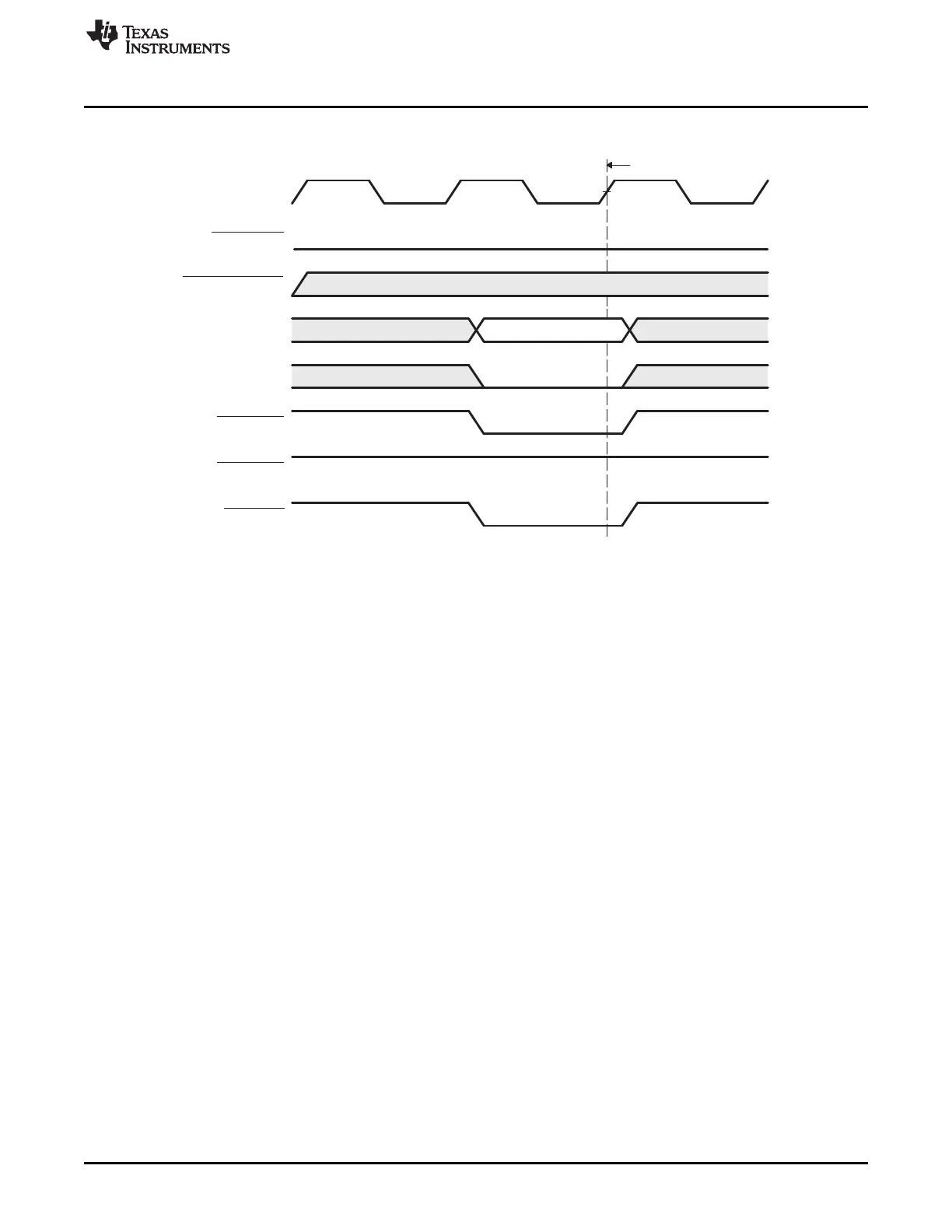
Figure 18-2. Timing Waveform of SDRAM PRE Command
18.2.4.2 Interfacing to SDRAM
The EMIFA supports a glueless interface to SDRAM devices with the following characteristics:
• Pre-charge bit is A[10]
• The number of column address bits is 8, 9, 10, or 11. See your device-specific data manual for the
number of column address bits supported on your device.
• The number of row address bits is 13, 14, 15, or 16. See your device-specific data manual for the
number of row address bits supported on your device.
• The number of internal banks is 1, 2, or 4. See your device-specific data manual for the number of
internal banks supported on your device.
Figure 18-3 shows an interface between the EMIFA and a 2M × 16 × 4 bank SDRAM device, and
Figure 18-4 shows an interface between the EMIFA and a 512K × 16 × 2 bank SDRAM device. For
devices supporting 16-bit interface, refer to Table 18-6 for list of commonly-supported SDRAM devices
and the required connections for the address pins.
 Loading...


