www.ti.com
SYSCFG Registers
189
SPRUH91D–March 2013–Revised September 2016
Submit Documentation Feedback
Copyright © 2013–2016, Texas Instruments Incorporated
System Configuration (SYSCFG) Module
10.5.10 Pin Multiplexing Control Registers (PINMUX0-PINMUX19)
NOTE: The C6745 DSP does not support all of the pins documented in the following subsections.
See the TMS320C6745/C6747 DSP Data Manual (SPRS377) for the peripherals supported.
Extensive use of pin multiplexing is used to accommodate the large number of peripheral functions in the
smallest possible package. On the device, pin multiplexing can be controlled on a pin by pin basis. This is
done by the pin multiplexing registers (PINMUX0-PINMUX19). Each pin that is multiplexed with several
different functions has a corresponding 4-bit field in PINMUXn. Pin multiplexing selects which of several
peripheral pin functions control the pins IO buffer output data and output enable values only. Note that the
input from each pin is always routed to all of the peripherals that share the pin; the PINMUX registers
have no effect on input from a pin. Hardware does not attempt to ensure that the proper pin multiplexing is
selected for the peripherals or that interface mode is being used. Detailed information about the pin
multiplexing and control is covered in the device-specific data manual. Access to the pin multiplexing utility
is available in OMAP-L137, TMS320C6747/6745/6743 Pin Multiplexing Utility Application Report
(SPRAB06).
10.5.10.1 Pin Multiplexing Control 0 Register (PINMUX0)
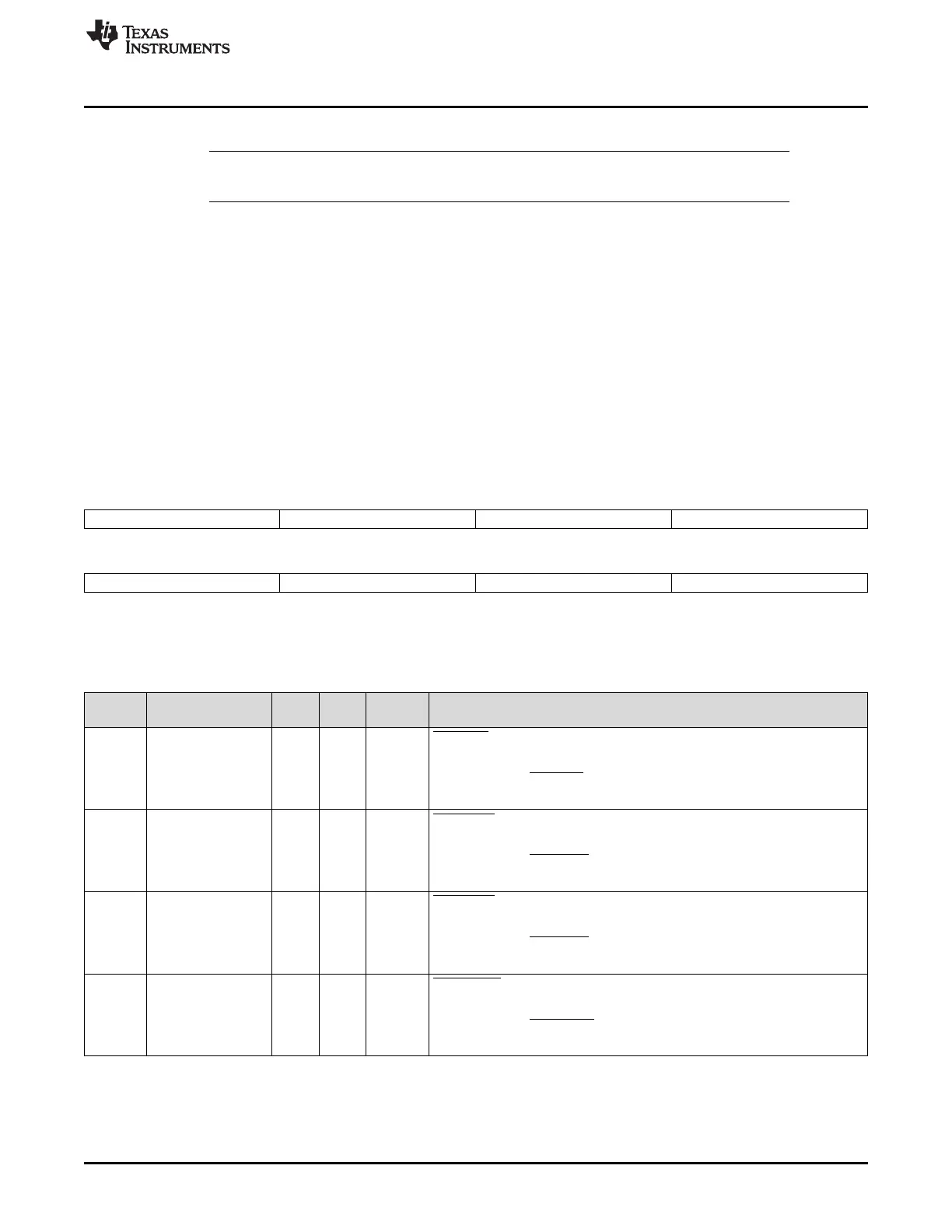
Figure 10-18. Pin Multiplexing Control 0 Register (PINMUX0)
31 28 27 24 23 20 19 16
PINMUX0_31_28 PINMUX0_27_24 PINMUX0_23_20 PINMUX0_19_16
R/W-0 R/W-0 R/W-0 R/W-0
15 12 11 8 7 4 3 0
PINMUX0_15_12 PINMUX0_11_8 PINMUX0_7_4 PINMUX0_3_0
R/W-0 R/W-0 R/W-0 R/W-0
LEGEND: R/W = Read/Write; -n = value after reset
(1)
The ZKB ball package is only available on the C6747 DSP; this package is not supported on the C6745 DSP.
(2)
The PTP pin package is only available on the C6745 DSP; this package is not supported on the C6747 DSP.
Table 10-22. Pin Multiplexing Control 0 Register (PINMUX0) Field Descriptions
Bit Field
ZKB
Ball
(1)
PTP
Pin
(2)
Value Description
31-28 PINMUX0_31_28 K15 59 EMB_WE Control
0 Pin is 3-stated.
1h Selects Function EMB_WE
2h-Fh Reserved
27-24 PINMUX0_27_24 A8 110 EMB_RAS Control
0 Pin is 3-stated.
1h Selects Function EMB_RAS
2h-Fh Reserved
23-20 PINMUX0_23_20 L13 57 EMB_CAS Control
0 Pin is 3-stated.
1h Selects Function EMB_CAS
2h-Fh Reserved
19-16 PINMUX0_19_16 D9 108 EMB_CS[0] Control
0 Pin is 3-stated.
1h Selects Function EMB_CS[0]
2h-Fh Reserved

 Loading...


