Architecture
www.ti.com
698
SPRUH91D–March 2013–Revised September 2016
Submit Documentation Feedback
Copyright © 2013–2016, Texas Instruments Incorporated
External Memory Interface A (EMIFA)
18.2.4 SDRAM Controller and Interface
The EMIFA can gluelessly interface to most standard SDR SDRAM devices and supports such features
as self refresh mode and prioritized refresh. In addition, it provides flexibility through programmable
parameters such as the refresh rate, CAS latency, and many SDRAM timing parameters. The following
sections include details on how to interface and properly configure the EMIFA to perform read and write
operations to externally connected SDR SDRAM devices. Also, Section 18.3 provides a detailed example
of interfacing the EMIFA to a common SDRAM device.
18.2.4.1 SDRAM Commands
The EMIFA supports the SDRAM commands described in Table 18-4. The truth table for the SDRAM
commands is shown in Table 18-5 and an example timing waveform of the PRE command is shown in
Figure 18-2. EMA_A[10] is pulled low in this example to deactivate only the bank specified by the
EMA_BA pins.
Table 18-4. EMIFA SDRAM Commands
Command Function
PRE Precharge. Depending on the value of EMA_A[10], the PRE command either deactivates the open row in all banks
(EMA_A[10] = 1) or only the bank specified by the EMA_BA[1:0] pins (EMA_A[10] = 0).
ACTV Activate. The ACTV command activates the selected row in a particular bank for the current access.
READ Read. The READ command outputs the starting column address and signals the SDRAM to begin the burst read
operation. Address EMA_A[10] is always pulled low to avoid auto precharge. This allows for better bank
interleaving performance.
WRT Write. The WRT command outputs the starting column address and signals the SDRAM to begin the burst write
operation. Address EMA_A[10] is always pulled low to avoid auto precharge. This allows for better bank
interleaving performance.
BT Burst terminate. The BT command is used to truncate the current read or write burst request.
LMR Load mode register. The LMR command sets the mode register of the attached SDRAM devices and is only
issued during the SDRAM initialization sequence described in Section 18.2.4.4.
REFR Auto refresh. The REFR command signals the SDRAM to perform an auto refresh according to its internal
address.
SLFR Self refresh. The self refresh command places the SDRAM into self refresh mode, during which it provides its own
clock signal and auto refresh cycles.
NOP No operation. The NOP command is issued during all cycles in which one of the above commands is not issued.
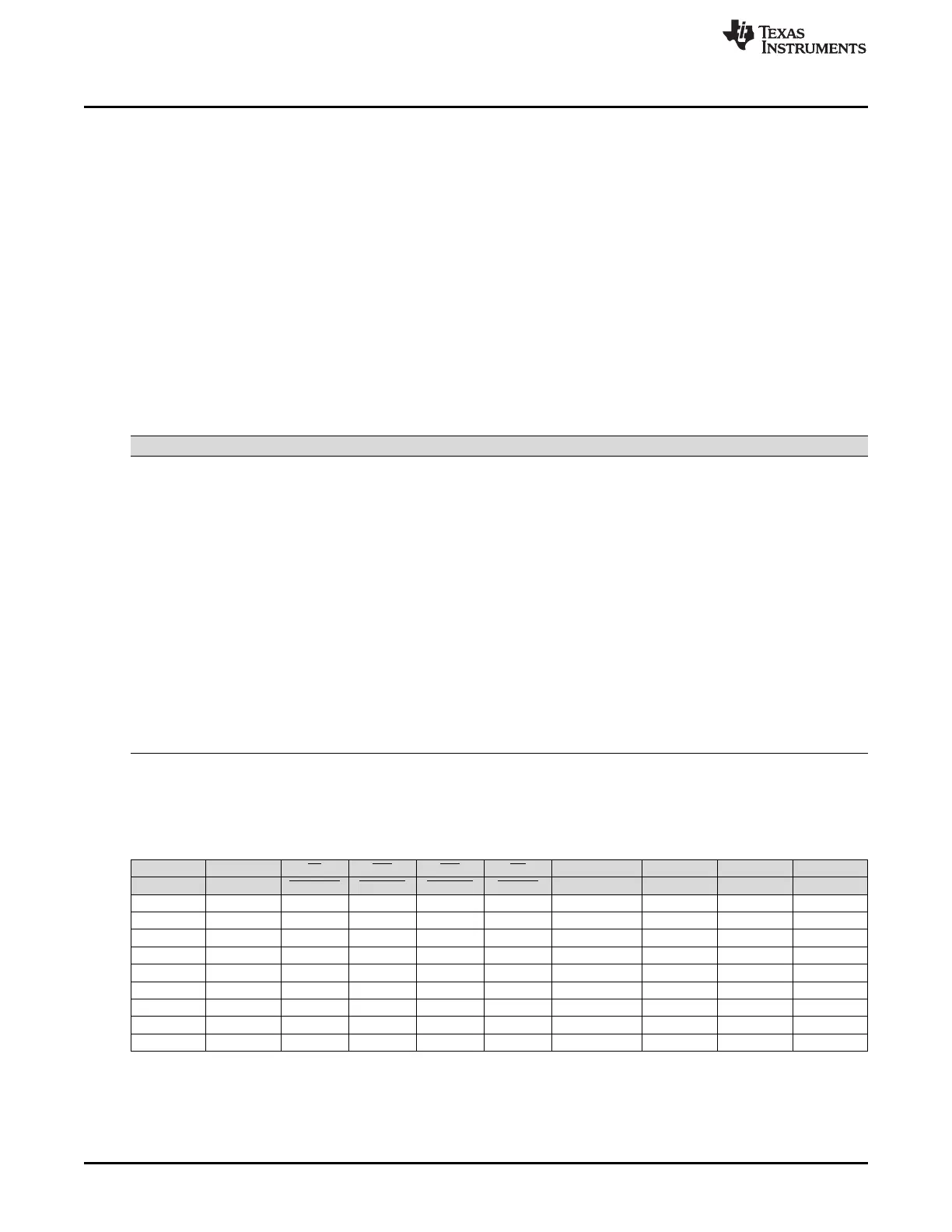
Table 18-5. Truth Table for SDRAM Commands
SDRAM Pins: CKE CS RAS CAS WE BA[1:0] A[12:11] A[10] A[9:0]
EMIFA Pins: EMA_SDCKE EMA_CS[0] EMA_RAS EMA_CAS EMA_WE EMA_BA[1:0] EMA_A[12:11] EMA_A[10] EMA_A[9:0]
PRE H L L H L Bank/X X L/H X
ACTV H L L H H Bank Row Row Row
READ H L H L H Bank Column L Column
WRT H L H L L Bank Column L Column
BT H L H H L X X X X
LMR H L L L L X Mode Mode Mode
REFR H L L L H X X X X
SLFR L L L L H X X X X
NOP H L H H H X X X X