www.ti.com
Registers
769
SPRUH91D–March 2013–Revised September 2016
Submit Documentation Feedback
Copyright © 2013–2016, Texas Instruments Incorporated
External Memory Interface A (EMIFA)
18.4.9 EMIFA Interrupt Masked Register (INTMSK)
Like the EMIFA interrupt raw register (INTRAW), the EMIFA interrupt masked register (INTMSK) is used to
monitor and clear the status of the EMIFA’s hardware-generated Asynchronous Timeout Interrupt. The
main difference between the two registers is that when the AT_MASKED bit in this register is set, an
active-high pulse will be sent to the CPU interrupt controller. Also, the AT_MASKED bit field in INTMSK is
only set to 1 if the associated interrupt has been enabled in the EMIFA interrupt mask set register
(INTMSKSET). The EMIFA on some devices does not have the EMA_WAIT pin, therefore, these registers
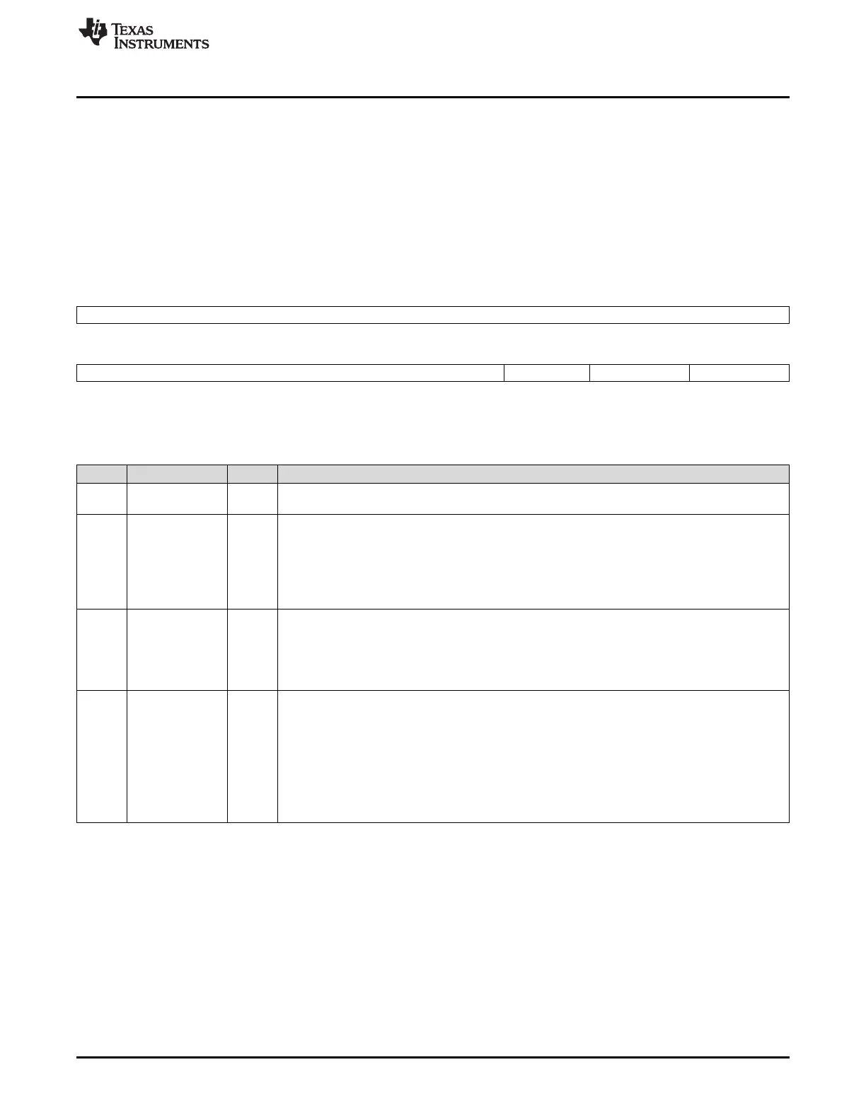
and fields are reserved on those devices. The INTMSK is shown in Figure 18-39 and described in
Table 18-57.
Figure 18-39. EMIFA Interrupt Mask Register (INTMSK)
31 8
Reserved
R-0
7 3 2 1 0
Reserved WR_MASKED LT_MASKED AT_MASKED
R-0 R/W1C-0 R/W1C-0 R/W1C-0
LEGEND: R/W = Read/Write; R = Read only; W1C = Write 1 to clear (writing 0 has no effect); -n = value after reset
Table 18-57. EMIFA Interrupt Mask Register (INTMSK) Field Descriptions
Bit Field Value Description
31-3 Reserved 0 Reserved. The reserved bit location is always read as 0. If writing to this field, always write the
default value of 0.
2 WR_MASKED Wait Rise Masked. This bit is set to 1 by hardware to indicate a rising edge has occurred on the
EMA_WAIT pin, provided that the WR_MASK_SET bit is set to 1 in the EMIFA interrupt mask set
register (INTMSKSET).
0 Indicates that a wait rise interrupt has not been generated. Writing a 0 has no effect.
1 Indicates that a wait rise interrupt has been generated. Writing a 1 will clear this bit and the WR bit
in the EMIFA interrupt raw register (INTRAW).
1 LT_MASKED Masked Line Trap. Set to 1 by hardware to indicate illegal memory access type or invalid cache line
size, only if the LT_MASK_SET bit in the EMIFA interrupt mask set register (INTMSKSET) is set to
1.
0 Writing a 0 has no effect.
1 Writing a 1 will clear this bit as well as the LT bit in the EMIFA interrupt raw register(INTRAW).
0 AT_MASKED Asynchronous Timeout Masked. This bit is set to 1 by hardware to indicate that during an extended
asynchronous memory access cycle, the EMA_WAIT pin did not go inactive within the number of
cycles defined by the MAX_EXT_WAIT field in the asynchronous wait cycle configuration register
(AWCC), provided that the AT_MASK_SET bit is set to 1 in the EMIFA interrupt mask set register
(INTMSKSET).
0 Indicates that an Asynchronous Timeout Interrupt has not been generated. Writing a 0 has no
effect.
1 Indicates that an Asynchronous Timeout Interrupt has been generated. Writing a 1 will clear this bit
as well as the AT bit in the EMIFA interrupt raw register (INTRAW).