www.ti.com
SYSCFG Registers
237
SPRUH91D–March 2013–Revised September 2016
Submit Documentation Feedback
Copyright © 2013–2016, Texas Instruments Incorporated
System Configuration (SYSCFG) Module
10.5.17 Chip Configuration 3 Register (CFGCHIP3)
The CFGCHIP3 register controls the following peripheral/module functions:
• DIV4p5 Clock Enable/Disable: The DIV4p5 (/4.5) hardware clock divider is provided to generate
133 MHz from the 600 MHz PLL clock for use as clocks to the EMIFs. Allows enabling/disabling this
clock divider.
• EMIFA Module Clock Source Control: Allows control for the source for the EMIFA module clock.
• EMIFB Memory Clock Source Control: Allows control for the source for the EMIFB SDRAM memory
clock.
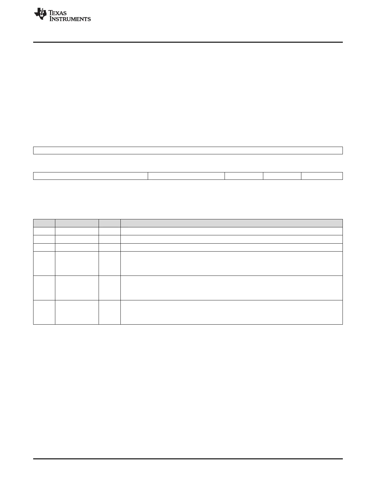
The CFGCHIP3 is shown in Figure 10-44 and described in Table 10-48.
Figure 10-44. Chip Configuration 3 Register (CFGCHIP3)
31 16
Reserved
R-0
15 8 7 3 2 1 0
Reserved Reserved DIV4P5ENA EMA_CLKSRC EMB_CLKSRC
R/W-FFh R/W-0 R/W-0 R/W-0 R/W-0
LEGEND: R/W = Read/Write; R = Read only; -n = value after reset
Table 10-48. Chip Configuration 3 Register (CFGCHIP3) Field Descriptions
Bit Field Value Description
31-16 Reserved 0 Reserved
15-8 Reserved FFh Reserved. Write the default value when modifying this register.
7-3 Reserved 0 Reserved. Write the default value to all bits when modifying this register.
2 DIV4P5ENA Controls the fixed DIV4.5 divider in the PLL controller.
0 Divide by 4.5 is disabled.
1 Divide by 4.5 is enabled.
1 EMA_CLKSRC Clock source for EMIFA clock domain.
0 Clock driven by PLLC SYSCLK3
1 Clock driven by DIV4.5 PLL output
0 EMB_CLKSRC Clock source for EMIFB clock domain.
0 Clock driven by PLLC SYSCLK5
1 Clock driven by DIV4.5 PLL output

 Loading...


