www.ti.com
SYSCFG Registers
207
SPRUH91D–March 2013–Revised September 2016
Submit Documentation Feedback
Copyright © 2013–2016, Texas Instruments Incorporated
System Configuration (SYSCFG) Module
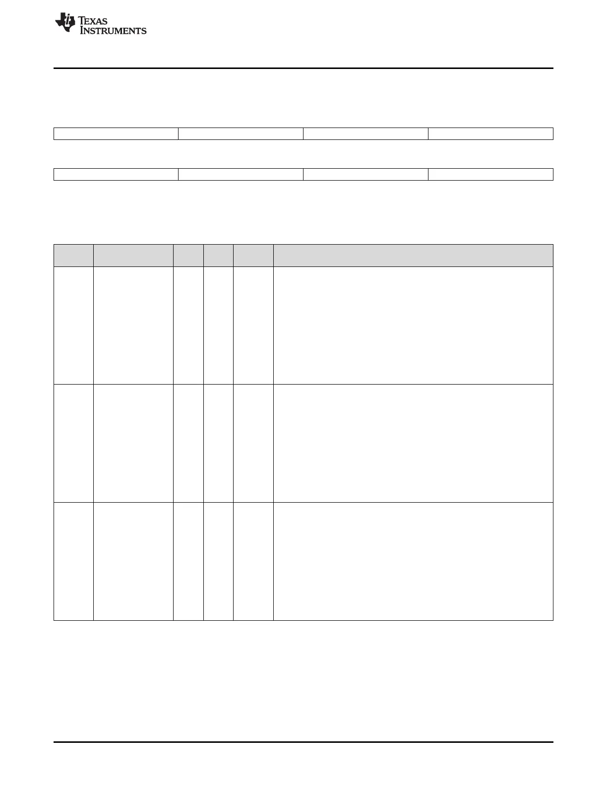
10.5.10.11 Pin Multiplexing Control 10 Register (PINMUX10)
Figure 10-28. Pin Multiplexing Control 10 Register (PINMUX10)
31 28 27 24 23 20 19 16
PINMUX10_31_28 PINMUX10_27_24 PINMUX10_23_20 PINMUX10_19_16
R/W-0 R/W-0 R/W-0 R/W-0
15 12 11 8 7 4 3 0
PINMUX10_15_12 PINMUX10_11_8 PINMUX10_7_4 PINMUX10_3_0
R/W-0 R/W-0 R/W-0 R/W-0
LEGEND: R/W = Read/Write; -n = value after reset
(1)
The ZKB ball package is only available on the C6747 DSP; this package is not supported on the C6745 DSP.
(2)
The PTP pin package is only available on the C6745 DSP; this package is not supported on the C6747 DSP.
Table 10-32. Pin Multiplexing Control 10 Register (PINMUX10) Field Descriptions
Bit Field
ZKB
Ball
(1)
PTP
Pin
(2)
Value Description
31-28 PINMUX10_31_28 D7 118 AXR0[6]/RMII_RXER[0]/ACLKR2/GP3[6] Control
0 Pin is 3-stated.
1h Selects Function AXR0[6]
2h Selects Function RMII_RXER[0]
3h Reserved
4h Selects Function ACLKR2
5h-7h Reserved
8h Selects Function GP3[6]
9h-Fh Reserved
27-24 PINMUX10_27_24 C7 117 AXR0[5]/RMII_RXD[1]/AFSX2/GP3[5] Control
0 Pin is 3-stated.
1h Selects Function AXR0[5]
2h Selects Function RMII_RXD[1]
3h Reserved
4h Selects Function AFSX2
5h-7h Reserved
8h Selects Function GP3[5]
9h-Fh Reserved
23-20 PINMUX10_23_20 B7 116 AXR0[4]/RMII_RXD[0]/AXR2[1]/GP3[4] Control
0 Pin is 3-stated.
1h Selects Function AXR0[4]
2h Selects Function RMII_RXD[0]
3h Reserved
4h Selects Function AXR2[1]
5h-7h Reserved
8h Selects Function GP3[4]
9h-Fh Reserved

 Loading...


