Registers
www.ti.com
960
SPRUH91D–March 2013–Revised September 2016
Submit Documentation Feedback
Copyright © 2013–2016, Texas Instruments Incorporated
Liquid Crystal Display Controller (LCDC)
23.3.8 LCD Raster Control Register (RASTER_CTRL)
The LCD raster control register (RASTER_CTRL) contains bit-fields that are used to control various
functions within the Raster controller sub-module. The RASTER_CTRL is shown in Figure 23-22 and
described in Table 23-18.
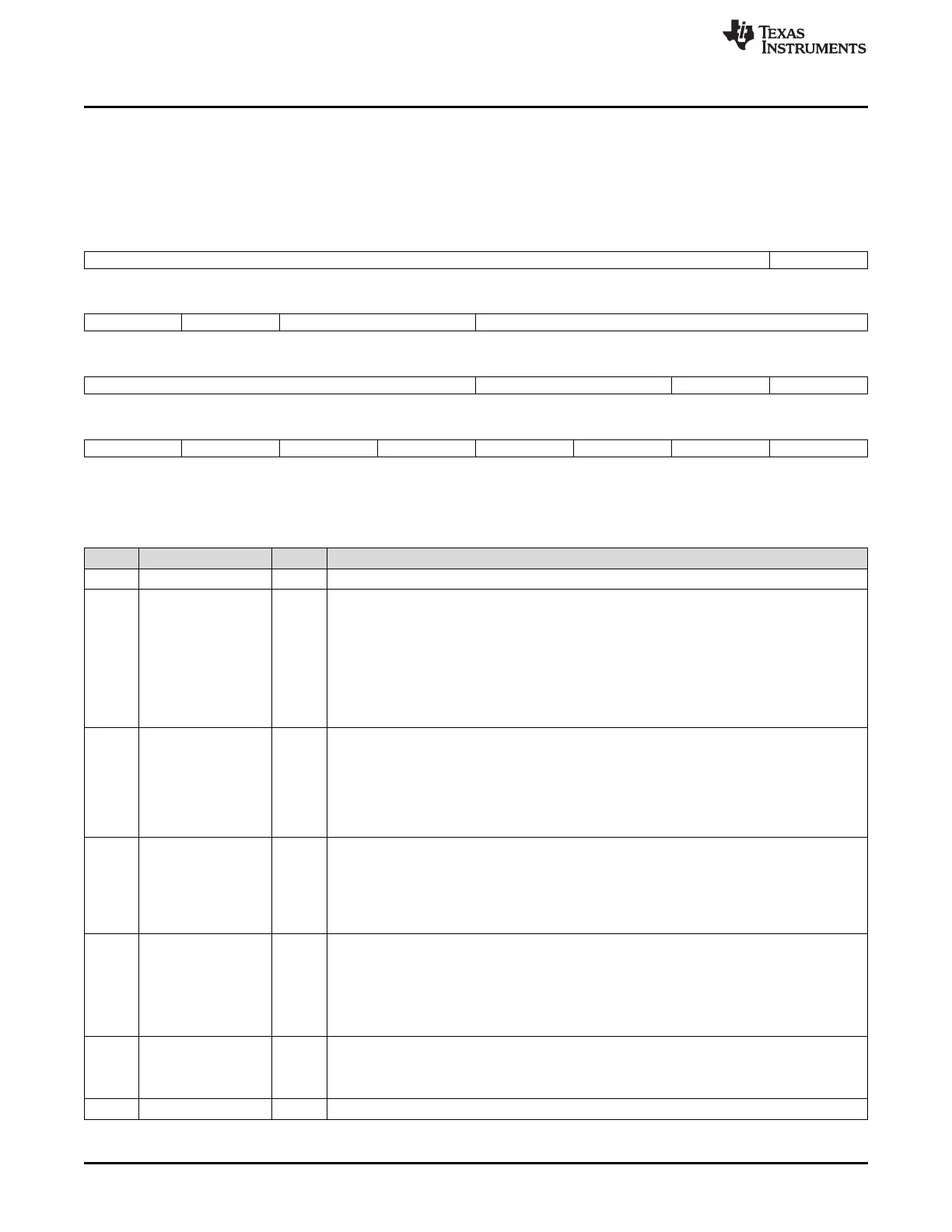
Figure 23-22. LCD Raster Control Register (RASTER_CTRL)
31 25 24
Reserved STN_565
R-0 R/W-0
23 22 21 20 19 16
TFT_ALT_MAP NIB_MODE PLM FIFO_DMA_DELAY
R/W-0 R/W-0 R/W-0 R/W-0
15 12 11 10 9 8
FIFO_DMA_DELAY Reserved MONO8B RD_ORDER
R/W-0 R-0 R/W-0 R/W-0
7 6 5 4 3 2 1 0
TFT_STN FUF_EN SL_EN PL_EN DONE_EN AC_EN MONO_COLOR RASTER_EN
R/W-0 R/W-0 R/W-0 R/W-0 R/W-0 R/W-0 R/W-0 R/W-0
LEGEND: R/W = Read/Write; R = Read only; -n = value after reset
Table 23-18. LCD Raster Control Register (RASTER_CTRL) Field Descriptions
Bit Field Value Description
31-25 Reserved 0 Reserved
24 STN_565 12-Bit-Per-Pixel (5-6-5) Mode.
This is only available in passive-color (STN) mode when 12 BPP is specified in the palette.
0 Disabled: The lower 12 bits of pixel data is processed and output; i.e., “X X X X R3 R2 R1 R0
G3 G2 G1 G0 B3 B2 B1 B0” (where X is ignored by the Raster Controller).
1 Enabled: Pixel data in the frame buffer is 16-bit but only 12 of the bits are processed and
output; i.e. “R3 R2 R1 R0 X G3 G2 G1 G0 X X B3 B2 B1 B0 X” (where X is ignored by the
Raster Controller).
The data patterns above refer to frame buffer bits not output bits.
23 TFT_ALT_MAP TFT Alternative Signal Mapping
0 Output pixel data for 1, 2, 4, and 8 BPP will be right aligned on LCD_D[11:0]. For example, “R3
R2 R1 R0 G3 G2 G1 G0 B3 B2 B1 B0”.
1 Output pixel data for 1, 2, 4, and 8 BPP will be converted to 5-6-5 format and transferred via
LCD_D[15:0]. For example, “R3 R2 R1 R0 R3 G3 G2 G1 G0 G3 G2 B3 B2 B1 B0 B3”.
The data patterns above refer to output bits not frame buffer bits.
22 NIB_MODE Nibble Mode
0 Nibble Mode disabled.
1 Nibble Mode enabled.
For 1, 2, and 4-BPP modes, this bit should be enabled.
For 8, 12, and 16-BPP modes, this bit should be disabled.
21-20 PLM 0-3h Palette Loading Mode
0 Palette and data.
1h Palette only.
2h Data only.
3h Do not use.
19-12 FIFO_DMA_DELAY 0-FFh FIFO DMA Request Delay. Encoded value used to specify the number of clocks the input FIFO
DMA request should be disabled. The delay clock count starts after 16 words are loaded into
the input FIFO.
Delay Time = [(LCD Pixel Clock) × FIFO_DMA_DELAY]
11-10 Reserved 0 Reserved