SYSCFG Registers
www.ti.com
230
SPRUH91D–March 2013–Revised September 2016
Submit Documentation Feedback
Copyright © 2013–2016, Texas Instruments Incorporated
System Configuration (SYSCFG) Module
10.5.14 Chip Configuration 0 Register (CFGCHIP0)
The chip configuration 0 register (CFGCHIP0) controls the following functions:
• PLL Controller memory-mapped register lock: Used to lock out writes to the PLL controller memory-
mapped registers (MMRs) to prevent any erroneous writes in software to the PLL controller register
space.
• EDMA3 Transfer Controller Default Burst Size (DBS) Control: This controls the maximum number of
bytes issued per read/write command or the burst size for the individual transfer controllers (TCs) on
the device. By default for all transfer controllers, the burst size is set to 16 bytes. However, CFGCHIP0
allows configurability of this parameter so that the TC can have a burst size of 16, 32, or 64 bytes. The
burst size determines the intra packet efficiency for the EDMA3 transfers. Additionally, it also facilitates
preemption at a system level, as all transfer requests are internally broken down by the transfer
controller up to DBS size byte chunks and on a system level, each master’s priority (configured by the
MSTPRI register) is evaluated at burst size boundaries. The DBS value can significantly impact the
standalone throughput performance depending on the source and destination (bus
width/frequency/burst support etc) and the TC FIFO size, etc. Therefore, the DBS size configuration
should be carefully analyzed to meet the system’s throughput/performance requirements.
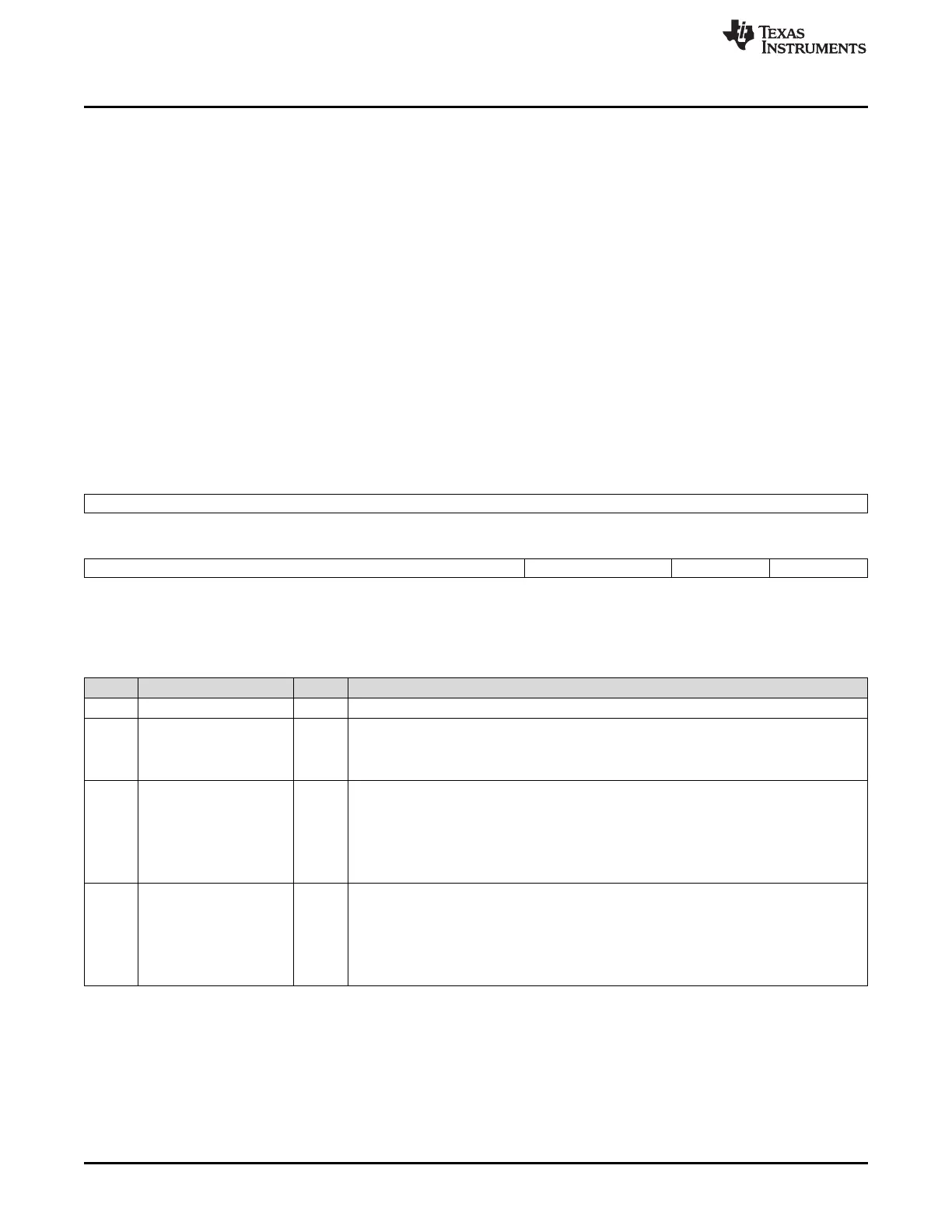
The CFGCHIP0 is shown in Figure 10-41 and described in Table 10-45.
Figure 10-41. Chip Configuration 0 Register (CFGCHIP0)
31 16
Reserved
R-0
15 5 4 3 2 1 0
Reserved PLL_MASTER_LOCK TC1DBS TC0DBS
R-0 R/W-0 R/W-0 R/W-0
LEGEND: R/W = Read/Write; R = Read only; -n = value after reset
Table 10-45. Chip Configuration 0 Register (CFGCHIP0) Field Descriptions
Bit Field Value Description
31-5 Reserved 0 Reserved
4 PLL_MASTER_LOCK PLL MMRs lock.
0 PLLC MMRs are freely accessible.
1 All PLLC MMRs are locked.
3-2 TC1DBS TC1 Default Burst Size (DBS).
0 16 bytes
1h 32 bytes
2h 64 bytes
3h Reserved
1-0 TC0DBS TC0 Default Burst Size (DBS).
0 16 bytes
1h 32 bytes
2h 64 bytes
3h Reserved



 To Next Page