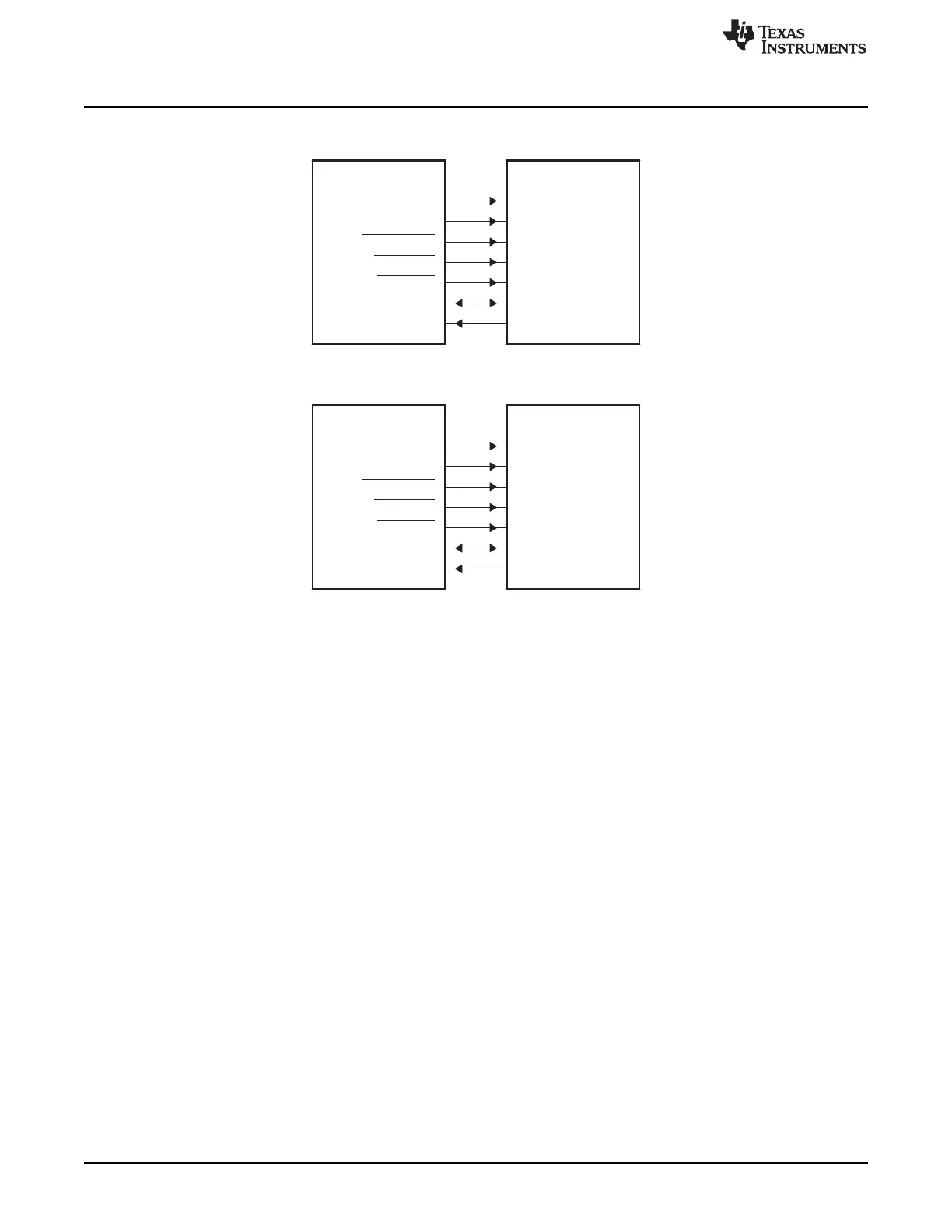
EMA_A[2]
EMA_A[1]
EMA_CS[n]
EMA_WE
EMA_OE
EMA_D[7:0]
EMA_WAIT
EMIFA
CLE
ALE
CE
WE
OE
IO[7:0]
R/B
NAND flash
a) Connection to 8−bit NAND device
b) Connection to 16−bit NAND device
EMA_WAIT
EMA_D[15:0]
EMA_OE
EMA_WE
EMA_CS[n]
EMA_A[1]
EMA_A[2]
EMIFA
CE
IO[15:0]
R/B
OE
WE
NAND flash
CLE
ALE
Architecture
www.ti.com
724
SPRUH91D–March 2013–Revised September 2016
Submit Documentation Feedback
Copyright © 2013–2016, Texas Instruments Incorporated
External Memory Interface A (EMIFA)
Figure 18-14. EMIFA to NAND Flash Interface
18.2.5.6.3 Driving CLE and ALE
As stated in Section 18.2.5.1, the EMIFA always drives the least significant bit of a 32-bit word address on
EMA_A[0]. This functionality must be considered when attempting to drive the offset lines connected to
CLE and ALE to the appropriate state.
For example, if using EMA_A[2] and EMA_A[1] to connect to CLE and ALE, respectively, the following
offsets should be added to EMIFA base address:
• 0000 0000h to drive CLE and ALE low
• 0000 0010h to drive CLE high and ALE low
• 0000 0008h to drive CLE low and ALE high
18.2.5.6.4 NAND Read and Program Operations
A NAND Flash access cycle is composed of a command, address, and data phase. The EMIFA will not
automatically generate these three phases to complete a NAND access with one transfer request. To
complete a NAND access cycle, multiple single asynchronous access cycles must be completed by the
EMIFA. Software must be used to request the appropriate asynchronous accesses to complete a NAND
Flash access cycle. This software must be developed to the specification of the chosen NAND Flash
device.
Since NAND operations are divided into single asynchronous access cycles, the chip select signal will not
remain activated for the duration of the NAND operation. Instead, the chip select signal will deactivate
between each asynchronous access cycle. For this reason, the EMIFA does not support NAND Flash
devices that require the chip select signal to remain low during the t
R
time for a read. See
Section 18.2.5.6.8 for workaround.



 To Next Page