EMB_CS
EMB_CAS
EMB_RAS
EMB_WE
EMB_CLK
EMB_SDCKE
EMB_BA[1:0]
EMB_A[11:0]
EMB_WE_DQM[3:0]
EMB_D[31:0]
EMIFB
CE
CAS
RAS
WE
CLK
CKE
BA[1:0]
A[11:0]
DQM[3:0]
DQ[31:0]
SDRAM
2Mx32x4
Bank
EMB_CS
EMB_CAS
EMB_RAS
EMB_WE
EMB_CLK
EMB_SDCKE
EMB_BA[1:0]
EMB_A[11:0]
EMB_WE_DQM[0]
EMB_WE_DQM[1]
EMB_D[15:0]
EMIFB
CE
CAS
RAS
WE
CLK
CKE
BA[1:0]
A[11:0]
LDQM
UDQM
DQ[15:0]
SDRAM
2Mx16x4
Bank
Architecture
www.ti.com
786
SPRUH91D–March 2013–Revised September 2016
Submit Documentation Feedback
Copyright © 2013–2016, Texas Instruments Incorporated
External Memory Interface B (EMIFB)
19.2.6.2 Interfacing to SDRAM
The EMIFB supports a glueless interface to SDRAM devices with the following characteristics:
• Pre-charge bit is A[10]
• The number of column address bits is 8, 9, 10 or 11
• The number of row address bits is 13(in case of mobile SDR, number of row address bits can be 9, 10,
11, 12, or 13)
• The number of internal banks is 1, 2 or 4
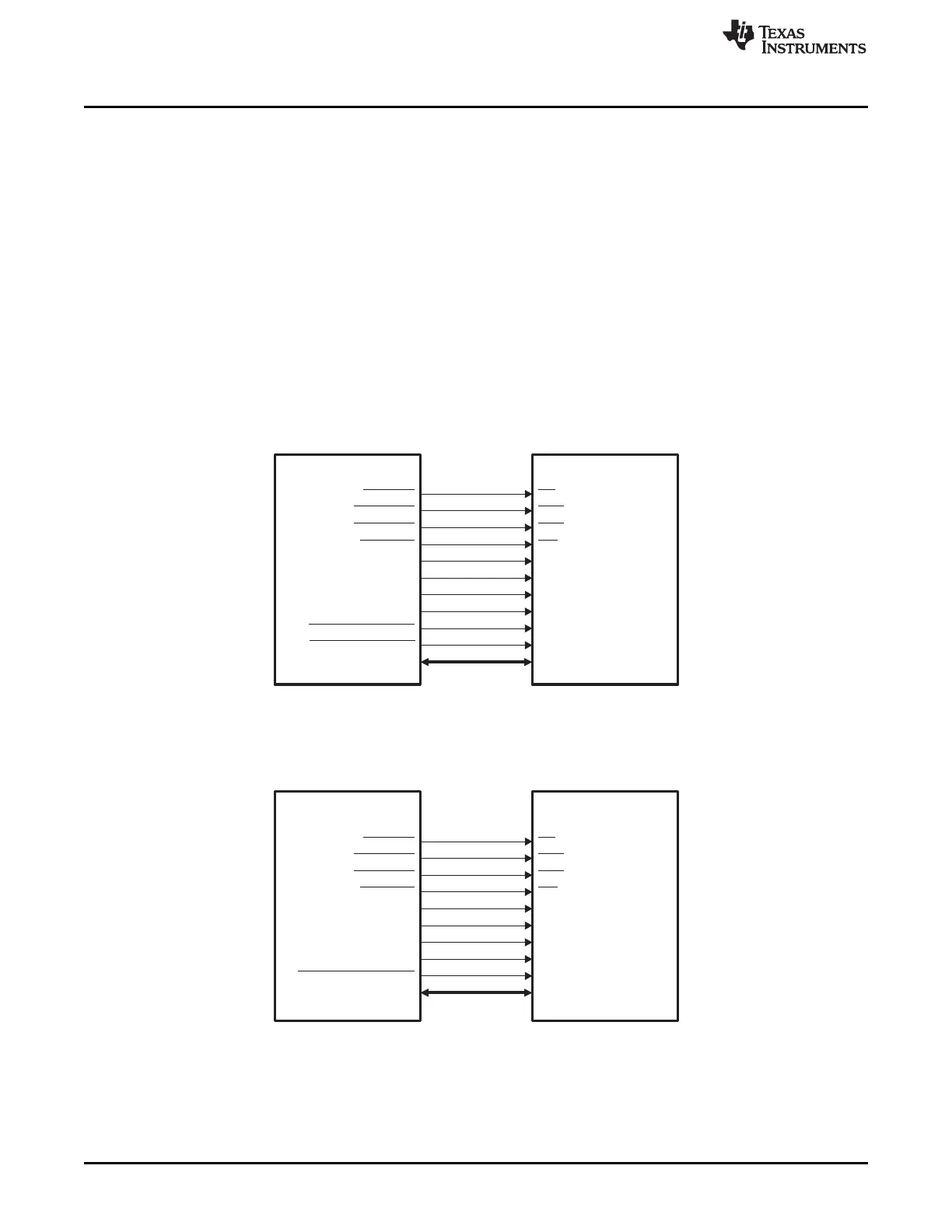
Figure 19-3 shows an interface between the EMIFB and a 2M × 16 × 4 bank SDRAM device. In addition,
Figure 19-4 shows an interface between the EMIFB and a 2M × 32 × 4 bank SDRAM device and
Figure 19-5 shows an interface between the EMIFB and two 4M × 16 × 4 bank SDRAM devices. Refer to
Table 19-4, as an example that shows additional list of commonly-supported SDRAM devices and the
required connections for the address pins. Note that in Table 19-4, page size/column size (not indicated in
the table) is varied to get the required addressability range.
Figure 19-3. EMIFB to 2M × 16 × 4 bank SDRAM Interface
Figure 19-4. EMIFB to 2M × 32 × 4 bank SDRAM Interface