Registers
www.ti.com
762
SPRUH91D–March 2013–Revised September 2016
Submit Documentation Feedback
Copyright © 2013–2016, Texas Instruments Incorporated
External Memory Interface A (EMIFA)
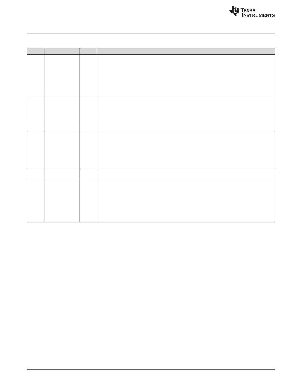
Table 18-51. SDRAM Configuration Register (SDCR) Field Descriptions (continued)
Bit Field Value Description
11-9 CL 0-7h CAS Latency. This field defines the CAS latency to be used when accessing connected SDRAM
devices. A 1 must be simultaneously written to the BIT11_9LOCK bit field of this register in order to
write to the CL bit field. Writing to this field triggers the SDRAM initialization sequence.
0-1h Reserved
2h CAS latency = 2 EMA_CLK cycles
3h CAS latency = 3 EMA_CLK cycles
4h-7h Reserved
8 BIT11_9LOCK Bits 11 to 9 lock. CL can only be written if BIT11_9LOCK is simultaneously written with a 1.
BIT11_9LOCK is always read as 0. Writing to this field triggers the SDRAM initialization sequence.
0 CL cannot be written.
1 CL can be written.
7 Reserved 0 Reserved. The reserved bit location is always read as 0. If writing to this field, always write the
default value of 0.
6-4 IBANK 0-7h Internal SDRAM Bank size. This field defines number of banks inside the connected SDRAM
devices. Writing to this field triggers the SDRAM initialization sequence.
0 1 bank SDRAM devices.
1 2 bank SDRAM devices.
2 4 bank SDRAM devices.
3h-7h Reserved.
3 Reserved 0 Reserved. The reserved bit location is always read as 0. If writing to this field, always write the
default value of 0.
2-0 PAGESIZE 0-7h Page Size. This field defines the internal page size of connected SDRAM devices. Writing to this
field triggers the SDRAM initialization sequence.
0 8 column address bits (256 elements per row)
1h 9 column address bits (512 elements per row)
2h 10 column address bits (1024 elements per row)
3h 11 column address bits (2048 elements per row)
4h-7h Reserved
 Loading...


