www.ti.com
Registers
811
SPRUH91D–March 2013–Revised September 2016
Submit Documentation Feedback
Copyright © 2013–2016, Texas Instruments Incorporated
External Memory Interface B (EMIFB)
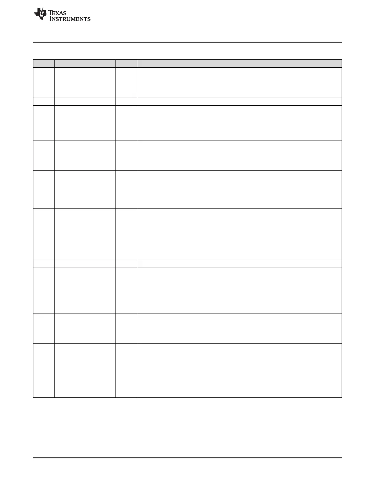
Table 19-25. SDRAM Configuration Register (SDCFG) Field Descriptions (continued)
Bit Field Value Description
23 BOOT_UNLOCK Boot unlock. Set to 1 to change the values of the fields that are affected by the
BOOT_UNLOCK bit. See the description of usage of the BOOT_UNLOCK bit.
0 The SDREN bit in this register may not be changed.
1 The SDREN bit in this register may be changed.
22-17 Reserved 0 All writes to these bit(s) must always have a value of 0.
16 SDREN SDRAM Enable. Active high bit which enables the SDRAM mode of the EMIFB controller.
This bit is writeable only when the BOOT_UNLOCK bit is unlocked.
0 SDRAM initialization and refreshes disabled, but SDRAM write/read transactions allowed.
This bit must not be cleared to 0 when EMIFB is in self-refresh state.
1 SDRAM fully enabled.
15 TIMUNLOCK Timing unlock. Controls the write permission settings for the SDRAM timing register 1
(SDTIM1) and SDRAM timing register 2 (SDTIM2).
0 CL bit in this register and register fields in SDTIM1 and SDTIM2 may not be changed.
1 CL bit in this register and register fields in SDTIM1 and SDTIM2 may be changed.
14 NM NM (Narrow mode). SDRAM data bus width. A write to this field will cause the EMIFB to
start the SDRAM initialization sequence.
0 32-bit SDR SDRAM
1 16-bit SDR SDRAM
13-12 Reserved 0 All writes to these bit(s) must always have a value of 0.
11-9 CL 0-7h CAS Latency. The value of this field defines the CAS latency to be used when accessing
connected SDRAM devices. A write to this field will cause the EMIFB to start the SDRAM
initialization sequence. This field is writeable only when the TIMUNLOCK bit is unlocked.
0-1h Reserved
2h CAS latency of 2
3h CAS latency of 3
4h-7h Reserved
8-7 Reserved 0 All writes to these bit(s) must always have a value of 0.
6-4 IBANK 0-7h Internal SDRAM Bank setup. Defines number of banks inside connected SDRAM devices. A
write to this field will cause the EMIFB to start the SDRAM initialization sequence.
0 1 bank SDRAM devices
1h 2 bank SDRAM devices
2h 4 bank SDRAM devices
3h-7h Reserved
3 EBANK External chip select setup. Always write 0 to this field. A write to this field will cause the
EMIFB to start the SDRAM initialization sequence.
0 Use EMB_CS for all SDRAM accesses.
1 Reserved
2-0 PAGESIZE 0-7h Page Size. Defines the internal page size of connected SDRAM devices. A write to this field
will cause the EMIFB to start the SDRAM initialization sequence.
0 256-word pages requiring 8 column address bits.
1h 512-word pages requiring 9 column address bits.
2h 1024-word pages requiring 10 column address bits.
3h 2048-word pages requiring 11 column address bits.
4h-7h Reserved



 To Next Page