General-Purpose Input/Output (GPIO)
www.ti.com
116
SPRUI07–March 2020
Submit Documentation Feedback
Copyright © 2020, Texas Instruments Incorporated
System Control and Interrupts
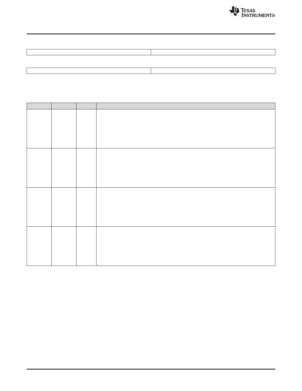
Figure 1-54. GPIO Port B Qualification Control (GPBCTRL) Register
31 24 23 16
QUALPRD3 QUALPRD2
R/W-0 R/W-0
15 8 7 0
QUALPRD1 QUALPRD0
R/W-0 R/W-0
LEGEND: R/W = Read/Write; R = Read only; -n = value after reset
(1)
This register is EALLOW protected. See Section 1.5.2 for more information.
(2)
T
SYSCLKOUT
indicates the period of SYSCLKOUT.
Table 1-57. GPIO Port B Qualification Control (GPBCTRL) Register Field Descriptions
Bits Field Value Description
(1)
31-24 QUALPRD3 Specifies the sampling period for pins GPIO56 to GPIO63
0x00 Sampling Period = T
SYSCLKOUT
(2)
0x01 Sampling Period = 2 × T
SYSCLKOUT
0x02 Sampling Period = 4 × T
SYSCLKOUT
. . . . . .
0xFF Sampling Period = 510 × T
SYSCLKOUT
23-16 QUALPRD2 Specifies the sampling period for pins GPIO48 to GPIO55
0x00 Sampling Period = T
SYSCLKOUT
(2)
0x01 Sampling Period = 2 × T
SYSCLKOUT
0x02 Sampling Period = 4 × T
SYSCLKOUT
. . . . . .
0xFF Sampling Period = 510 × T
SYSCLKOUT
15-8 QUALPRD1 Specifies the sampling period for pins GPIO40 to GPIO47
0x00 Sampling Period = T
SYSCLKOUT
(2)
0x01 Sampling Period = 2 × T
SYSCLKOUT
0x02 Sampling Period = 4 × T
SYSCLKOUT
. . . . . .
0xFF Sampling Period = 510 × T
SYSCLKOUT
7-0 QUALPRD0 Specifies the sampling period for pins GPIO32 to GPIO39
0x00 Sampling Period = T
SYSCLKOUT
(2)
0x01 Sampling Period = 2 × T
SYSCLKOUT
0x02 Sampling Period = 4 × T
SYSCLKOUT
. . . . . .
0xFF Sampling Period = 510 × T
SYSCLKOUT
 Loading...