Write to DXR1DXR1 to XSR1 copy(C)Write to DXR1(C)DXR1 to XSR1 copy(B)
XRDY
DX
FSX
CLKX
C5C6C7B0B1B2B3B4B5B6B7A0A1
DXR[1,2]
From CPU or
DMA controller
Compress
do not modify
or
www.ti.com
McBSP Operation
669
SPRUI07–March 2020
Submit Documentation Feedback
Copyright © 2020, Texas Instruments Incorporated
Multichannel Buffered Serial Port (McBSP)
RBR2 and RBR1 are used and RBR2 contains the most significant bits.
5. The McBSP copies the contents of the receive buffer register(s) into the data receive register(s),
provided that DRR1 is not full with previous data. When DRR1 receives new data, the receiver ready
bit (RRDY) is set in SPCR1. This indicates that received data is ready to be read by the CPU or the
DMA controller.
If the word length is 16 bits or smaller, only DRR1 is used. If the word length is larger than 16 bits,
DRR2 and DRR1 are used and DRR2 contains the most significant bits.
If companding is used during the copy (RCOMPAND = 10b or 11b in RCR2), the 8-bit compressed
data in RBR1 is expanded to a left-justified 16-bit value in DRR1. If companding is disabled, the data
copied from RBR[1,2] to DRR[1,2] is justified and bit filled according to the RJUST bits.
6. The CPU or the DMA controller reads the data from the data receive register(s). When DRR1 is read,
RRDY is cleared and the next RBR-to-DRR copy is initiated.
NOTE: If both DRRs are required (word length larger than 16 bits), the CPU or the DMA controller
must read from DRR2 first and then from DRR1. As soon as DRR1 is read, the next RBR-to-
DRR copy is initiated. If DRR2 is not read first, the data in DRR2 is lost.
When activity is not properly timed, errors can occur. See the following topics for more details:
• Overrun in the Receiver (see Section 12.5.2)
• Unexpected Receive Frame-Synchronization Pulse (see Section 12.5.3)
12.3.6 McBSP Transmission
This section explains the fundamental process of transmission in the McBSP. For details about how to
program the McBSP transmitter, see Section 12.9.
Figure 12-15 and Figure 12-16 show how transmission occurs in the McBSP. Figure 12-15 shows the
physical path for the data. Figure 12-16 is a timing diagram showing signal activity for one possible
transmission scenario. A description of the process follows the figures.
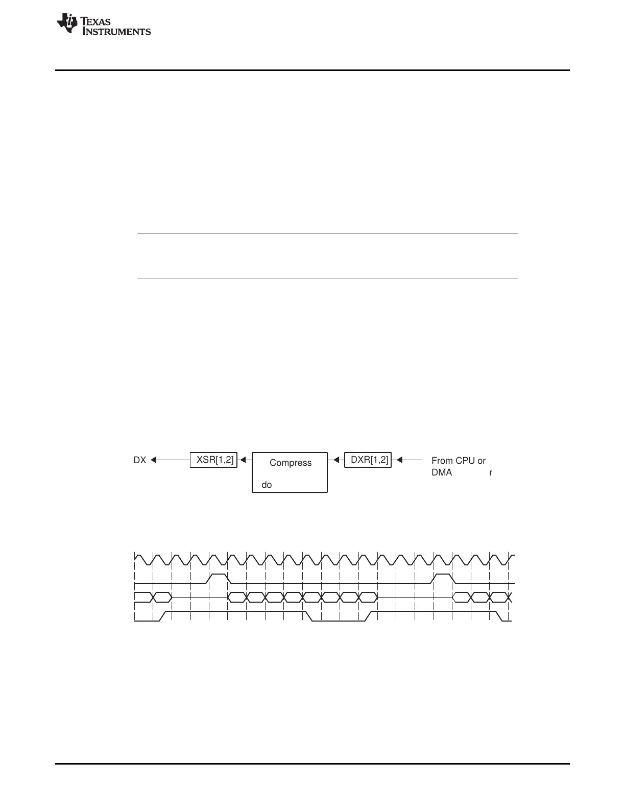
Figure 12-15. McBSP Transmission Physical Data Path
A XSR[1,2]: Transmit shift registers 1 and 2
B DXR[1,2]: Data transmit registers 1 and 2
Figure 12-16. McBSP Transmission Signal Activity
A CLKX: Internal transmit clock
B FSX: Internal transmit frame-synchronization signal
C DX: Data on DX pin
D XRDY: Status of transmitter ready bit (high is 1)
1. The CPU or the DMA controller writes data to the data transmit register(s). When DXR1 is loaded, the
transmitter ready bit (XRDY) is cleared in SPCR2 to indicate that the transmitter is not ready for new
data.
If the word length is 16 bits or smaller, only DXR1 is used. If the word length is larger than 16 bits,
DXR2 and DXR1 are used and DXR2 contains the most significant bits. For details on choosing a word
 Loading...