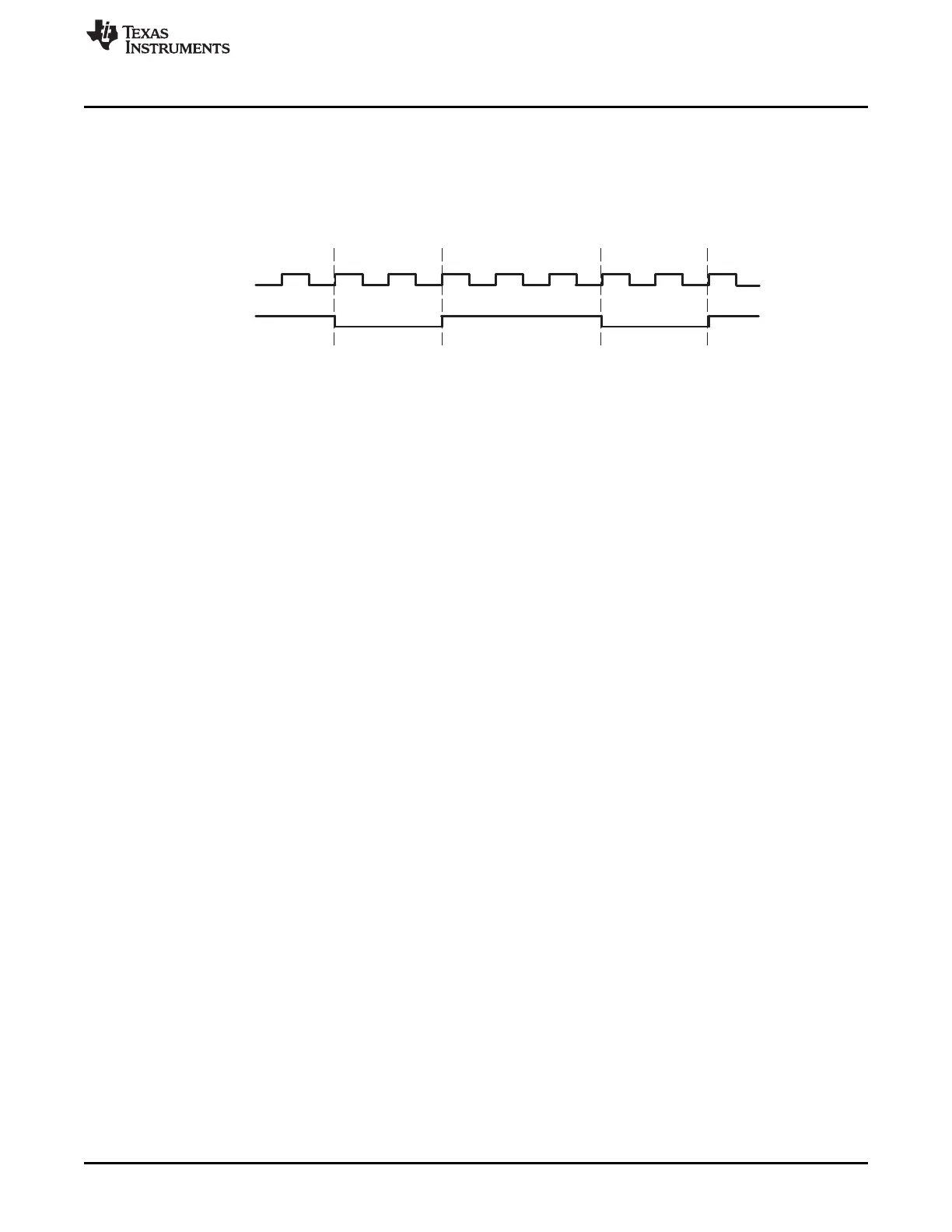
LSPCLK
SPICLK
2 cycles 3 cycles 2 cycles
www.ti.com
SPI Operation
559
SPRUI07–March 2020
Submit Documentation Feedback
Copyright © 2020, Texas Instruments Incorporated
Serial Peripheral Interface (SPI)
SPICLK symmetry is retained only when the result of (SPIBRR+1) is an even value. When (SPIBRR + 1)
is an odd value and SPIBRR is greater than 3, SPICLK becomes asymmetrical. The low pulse of SPICLK
is one LSPCLK cycle longer than the high pulse when CLKPOLARITY bit is clear (0). When
CLKPOLARITY bit is set to 1, the high pulse of the SPICLK is one LSPCLK cycle longer than the low
pulse, as shown in Figure 9-6.
Figure 9-6. SPI: SPICLK-LSPCLK Characteristic When (BRR + 1) is Odd, BRR > 3, and CLKPOLARITY = 1
9.3.7 SPI FIFO Description
The following steps explain the FIFO features and help with programming the SPI FIFOs:
1. Reset. At reset the SPI powers up in standard SPI mode and the FIFO function is disabled. The FIFO
registers SPIFFTX, SPIFFRX and SPIFFCT remain inactive.
2. Standard SPI. The standard 28x SPI mode will work with SPIINT/SPIRXINT as the interrupt source.
3. Mode change. FIFO mode is enabled by setting the SPIFFENA bit to 1 in the SPIFFTX register.
SPIRST can reset the FIFO mode at any stage of its operation.
4. Active registers. All the SPI registers and SPI FIFO registers SPIFFTX, SPIFFRX, and SPIFFCT will
be active.
5. Interrupts. FIFO mode has two interrupts one for the transmit FIFO, SPITXINT and one for the receive
FIFO, SPIRXINT. SPIRXINT is the common interrupt for SPI FIFO receive, receive error and receive
FIFO overflow conditions. The single SPIINT for both transmit and receive sections of the standard SPI
will be disabled and this interrupt will service as SPI receive FIFO interrupt. For more information, refer
to Section 9.2.3
6. Buffers. Transmit and receive buffers are each supplemented with a 16 word FIFO. The one-word
transmit buffer (SPITXBUF) of the standard SPI functions as a transition buffer between the transmit
FIFO and shift register. The one-word transmit buffer will be loaded from transmit FIFO only after the
last bit of the shift register is shifted out.
7. Delayed transfer. The rate at which transmit words in the FIFO are transferred to transmit shift
register is programmable. The SPIFFCT register bits (7−0) FFTXDLY7−FFTXDLY0 define the delay
between the word transfer. The delay is defined in number SPI serial clock cycles. The 8-bit register
could define a minimum delay of 0 SPICLK cycles and a maximum of 255 SPICLK cycles. With zero
delay, the SPI module can transmit data in continuous mode with the FIFO words shifting out back to
back. With the 255 clock delay, the SPI module can transmit data in a maximum delayed mode with
the FIFO words shifting out with a delay of 255 SPICLK cycles between each words. The
programmable delay facilitates glueless interface to various slow SPI peripherals, such as EEPROMs,
ADC, DAC, and so on.
8. FIFO status bits. Both transmit and receive FIFOs have status bits TXFFST or RXFFST that define
the number of words available in the FIFOs at any time. The transmit FIFO reset bit (TXFIFO) and
receive reset bit (RXFIFO) will reset the FIFO pointers to zero when these bits are set to 1. The FIFOs
will resume operation from start once these bits are cleared to zero.
9. Programmable interrupt levels. Both transmit and receive FIFOs can generate CPU interrupts. The
transmit interrupt (SPITXINT) is generated whenever the transmit FIFO status bits (TXFFST) match
(less than or equal to) the interrupt trigger level bits (TXFFIL). The receive interrupt (SPIRXINT) is
generated whenever the receive FIFO status bits (RXFFST) match (greater than or equal to) the
interrupt trigger level RXFFIL. This provides a programmable interrupt trigger for transmit and receive
sections of the SPI. The default value for these trigger level bits will be 0x11111 for receive FIFO and
0x00000 for transmit FIFO, respectively.
 Loading...