DX
DR
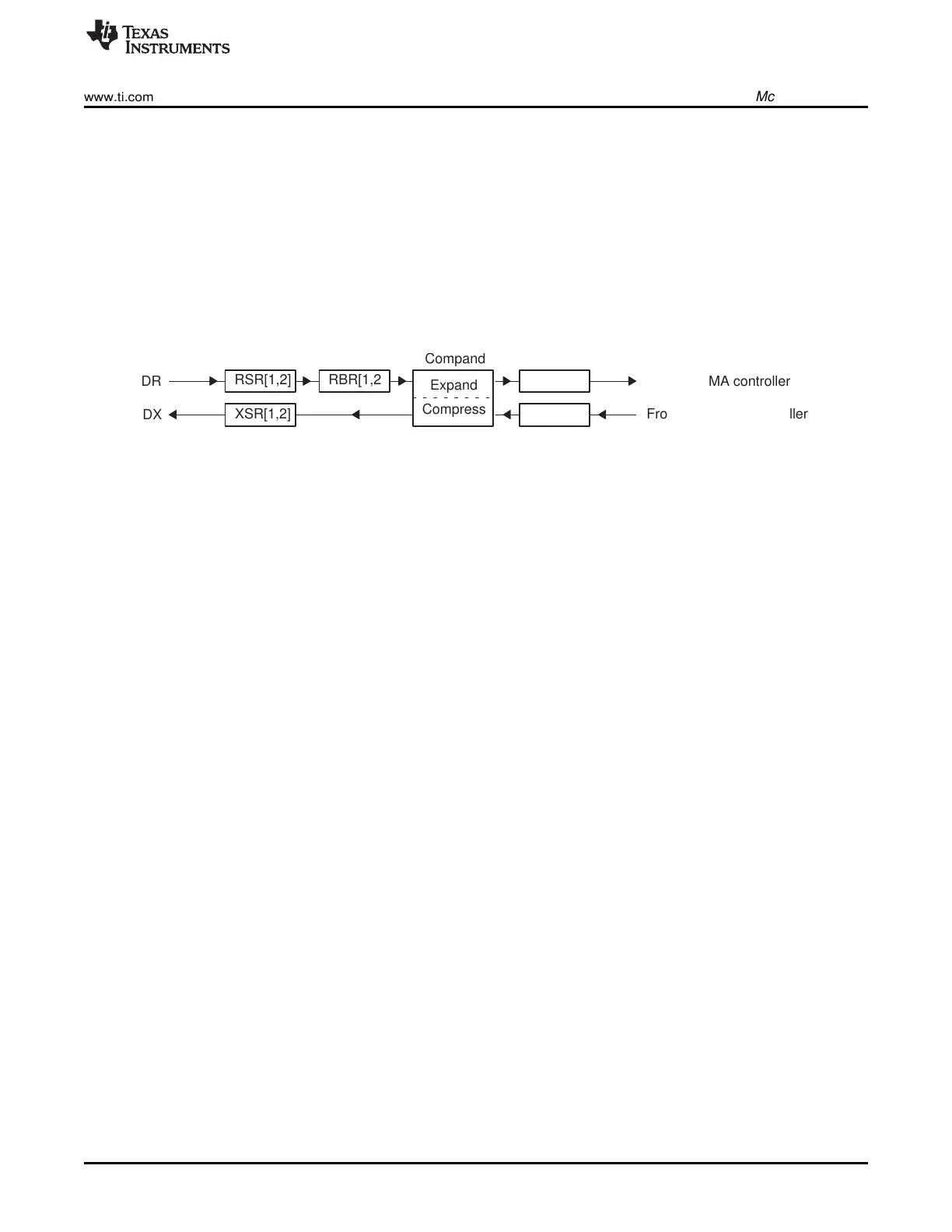
Compand
RSR[1,2]
Compress
Expand
XSR[1,2]
DXR[1,2]
DRR[1,2]RBR[1,2]
To CPU/DMA controller
From CPU/DMA controller
www.ti.com
McBSP Operation
661
SPRUI07–March 2020
Submit Documentation Feedback
Copyright © 2020, Texas Instruments Incorporated
Multichannel Buffered Serial Port (McBSP)
• Frame phases
• McBSP reception
• McBSP transmission
• Interrupts and DMA events generated by McBSPs
12.3.1 Data Transfer Process of McBSPs
Figure 12-2 shows a diagram of the McBSP data transfer paths. The McBSP receive operation is triple-
buffered, and transmit operation is double-buffered. The use of registers varies, depending on whether the
defined length of each serial word is 16 bits.
Figure 12-2. McBSP Data Transfer Paths
12.3.1.1 Data Transfer Process for Word Length of 8, 12, or 16 Bits
If the word length is 16 bits or smaller, only one 16-bit register is needed at each stage of the data transfer
paths. The registers DRR2, RBR2, RSR2, DXR2, and XSR2 are not used (written, read, or shifted).
Receive data arrives on the DR pin and is shifted into receive shift register 1 (RSR1). Once a full word is
received, the content of RSR1 is copied to the receive buffer register 1 (RBR1), that is, if RBR1 is not full
with previous data. RBR1 is then copied to the data receive register 1 (DRR1), unless the previous
content of DRR1 has not been read by the CPU or the DMA controller. If the companding feature of the
McBSP is implemented, the required word length is 8 bits and receive data is expanded into the
appropriate format before being passed from RBR1 to DRR1. For more details about reception, see
Section 12.3.5.
Transmit data is written by the CPU or the DMA controller to the data transmit register 1 (DXR1). If there
is no previous data in the transmit shift register (XSR1), the value in DXR1 is copied to XSR1; otherwise,
DXR1 is copied to XSR1 when the last bit of the previous data is shifted out on the DX pin. If selected, the
companding module compresses 16-bit data into the appropriate 8-bit format before passing it to XSR1.
After transmit frame synchronization, the transmitter begins shifting bits from XSR1 to the DX pin. For
more details about transmission, see Section 12.3.6.
12.3.1.2 Data Transfer Process for Word Length of 20, 24, or 32 Bits
If the word length is larger than 16 bits, two 16-bit registers are needed at each stage of the data transfer
paths. The registers DRR2, RBR2, RSR2, DXR2, and XSR2 are needed to hold the most significant bits.
Receive data arrives on the DR pin and is shifted first into RSR2 and then into RSR1. Once the full word
is received, the contents of RSR2 and RSR1 are copied to RBR2 and RBR1, respectively, if RBR1 is not
full. Then the contents of RBR2 and RBR1 are copied to DRR2 and DRR1, respectively, unless the
previous content of DRR1 has not been read by the CPU or the DMA controller. The CPU or the DMA
controller must read data from DRR2 first and then from DRR1. When DRR1 is read, the next RBR-to-
DRR copy occurs. For more details about reception, see Section 12.3.5.
For transmission, the CPU or the DMA controller must write data to DXR2 first and then to DXR1. When
new data arrives in DXR1, if there is no previous data in XSR1, the contents of DXR2 and DXR1 are
copied to XSR2 and XSR1, respectively; otherwise, the contents of the DXRs are copied to the XSRs
when the last bit of the previous data is shifted out on the DX pin. After transmit frame synchronization,
the transmitter begins shifting bits from the XSRs to the DX pin. For more details about transmission, see
Section 12.3.6.
 Loading...