FSR
GSYNC
synchronization
andclock
detection
Framepulse
SRGR1
[CLKGDV]
CLKSRG
0
1
CLKXP
MCLKXpin
CLKRP
MCLKRpin
0
1
LSPCLK
SRGR2[CLKSM]
0
1
PCR
[SCLKSME]
SRGR1
[FWID]
CLKG
FSG
pulse
Frame
SRGR2
[FPER]
÷
Reserved
/(CLKGDV+1)
www.ti.com
McBSP Sample Rate Generator
671
SPRUI07–March 2020
Submit Documentation Feedback
Copyright © 2020, Texas Instruments Incorporated
Multichannel Buffered Serial Port (McBSP)
12.4.1 Block Diagram
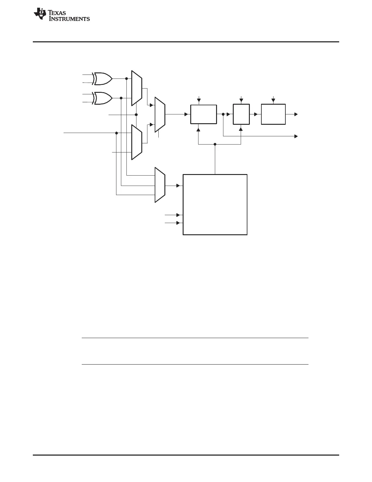
Figure 12-17. Conceptual Block Diagram of the Sample Rate Generator
The source clock for the sample rate generator (labeled CLKSRG in the diagram) can be supplied by the
LSPCLK, or by an external pin (MCLKX or MCLKR ). The source is selected with the SCLKME bit of PCR
and the CLKSM bit of SRGR2. If a pin is used, the polarity of the incoming signal can be inverted with the
appropriate polarity bit (CLKXP of PCR or CLKRP of PCR).
The sample rate generator has a three-stage clock divider that gives CLKG and FSG programmability.
The three stages provide:
• Clock divide-down. The source clock is divided according to the CLKGDV bits of SRGR1 to produce
CLKG.
• Frame period divide-down. CLKG is divided according to the FPER bits of SRGR2 to control the period
from the start of a frame-pulse to the start of the next pulse.
• Frame-synchronization pulse-width countdown. CLKG cycles are counted according to the FWID bits
of SRGR1 to control the width of each frame-synchronization pulse.
NOTE: The McBSP cannot operate at a frequency faster than ½ the source clock frequency. You
must choose an input clock frequency and a CLKGDV value such that CLKG is less than or
equal to ½ the source clock frequency.
In addition to the three-stage clock divider, the sample rate generator has a frame-synchronization pulse
detection and clock synchronization module that allows synchronization of the clock divide down with an
incoming frame-synchronization pulse on the FSR pin. This feature is enabled or disabled with the
GSYNC bit of SRGR2.
For details on getting the sample rate generator ready for operation, see Section 12.4.4.
 Loading...