CLKG frequency +
Input clock frequency
(
CLKGDV ) 1
)
CLKSRG
0
1
CLKXP
MCLKXpin
CLKRP
MCLKRpin
0
1
LSPCLK
CLKSM
0
1
SCLKME
Toclockdividers
Reserved
www.ti.com
McBSP Sample Rate Generator
673
SPRUI07–March 2020
Submit Documentation Feedback
Copyright © 2020, Texas Instruments Incorporated
Multichannel Buffered Serial Port (McBSP)
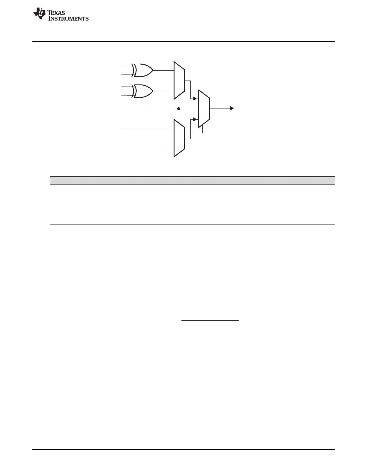
Figure 12-18. Possible Inputs to the Sample Rate Generator and the Polarity Bits
Table 12-6. Polarity Options for the Input to the Sample Rate Generator
Input Clock Polarity Option Effect
LSPCLK Always positive polarity Rising edge of CPU clock generates transitions on CLKG and FSG.
Signal on MCLKR pin CLKRP = 0 in PCR Falling edge on MCLKR pin generates transitions on CLKG and FSG.
CLKRP = 1 in PCR Rising edge on MCLKR pin generates transitions on CLKG and FSG.
Signal on MCLKX pin CLKXP = 0 in PCR Rising edge on MCLKX pin generates transitions on CLKG and FSG.
CLKXP = 1 in PCR Falling edge on MCLKX pin generates transitions on CLKG and FSG.
12.4.1.4 Choosing a Frequency for the Output Clock (CLKG)
The input clock (LSPCLK or external clock) can be divided down by a programmable value to drive CLKG.
Regardless of the source to the sample rate generator, the rising edge of CLKSRG (see Figure 12-1)
generates CLKG and FSG.
The first divider stage of the sample rate generator creates the output clock from the input clock. This
divider stage uses a counter that is preloaded with the divide down value in the CLKGDV bits of SRGR1.
The output of this stage is the data clock (CLKG). CLKG has the frequency represented by the equation
below.
Equation 1: CLKG Frequency
12.4.1.4.1 CLKG Frequency
Thus, the input clock frequency is divided by a value between 1 and 256. When CLKGDV is odd or equal
to 0, the CLKG duty cycle is 50%. When CLKGDV is an even value, 2p, representing an odd divide down,
the high-state duration is p+1 cycles and the low-state duration is p cycles.
12.4.1.5 Keeping CLKG Synchronized to External MCLKR
When the MCLKR pin is used to drive the sample rate generator (see Section 12.4.1.2), the GSYNC bit in
SRGR2 and the FSR pin can be used to configure the timing of the output clock (CLKG) relative to the
input clock. Note that this feature is available only when the MCLKR pin is used to feed the external clock.
GSYNC = 1 ensures that the McBSP and an external device are dividing down the input clock with the
same phase relationship. If GSYNC = 1, an inactive-to-active transition on the FSR pin triggers a
resynchronization of CLKG and generation of FSG.
For more details about synchronization, see Section 12.4.3.
 Loading...