1
0
/2
SYSCLKOUT
C28x
CPU
XINTCNF2(XTIMCLK)
1
0
/2
XTIMCLK
XINTCNF2
(CLKMODE)
XINTCNF2
(CLKOFF)
0
1
0
XCLKOUT
XTIMING0
XTIMING6
XTIMING7
XBANK
LEAD/ACTIVE/TRAIL
PCLKR3[XINTFENCLK]
XINTF Configuration Overview
www.ti.com
840
SPRUI07–March 2020
Submit Documentation Feedback
Copyright © 2020, Texas Instruments Incorporated
External Interface (XINTF)
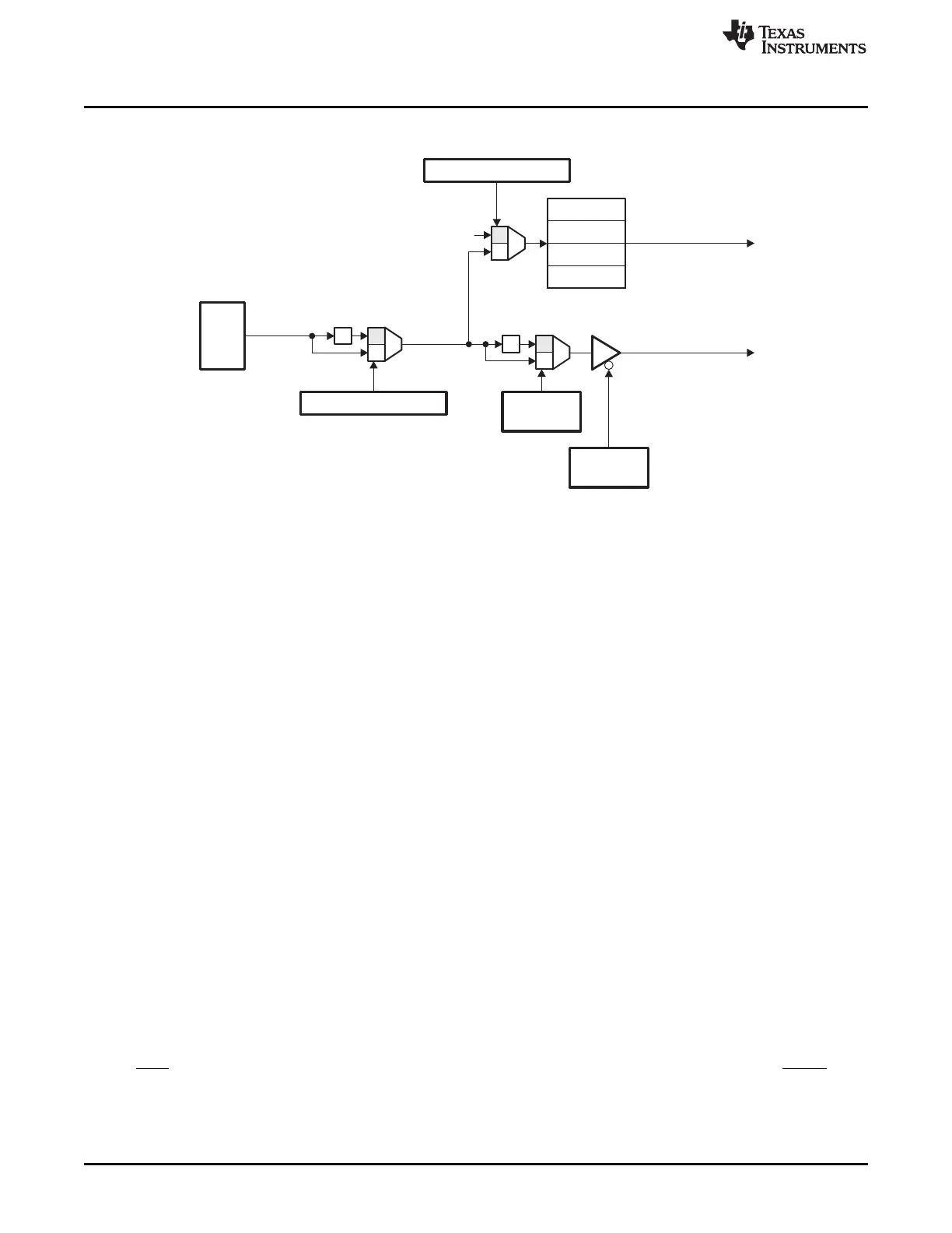
Figure 14-3. Relationship Between XTIMCLK and SYSCLKOUT
All accesses to all of the XINTF zones are based on the frequency of the internal XINTF clock, XTIMCLK.
XTIMCLK can be configured to be either equal or one half of SYSCLKOUT by writing to the XTIMCLK bit
in the XINTFCNF2 register. By default XTIMCLK is one-half of SYSCLKOUT.
All XINTF accesses begin on the rising edge of the external clock out, XCLKOUT. In addition, external
logic may be clocked off of XCLKOUT. The frequency of XCLKOUT can be configured as a ratio of the
internal XINTF clock, XTIMCLK. XCLKOUT can be configured to be either equal or one-half of XTIMCLK
by writing to the CLKMODE bit in the XINTFCNF2 register. By default, XCLKOUT is one-half of XTIMCLK,
or one-fourth of the CPU clock, SYSCLKOUT.
To reduce system noise, the XCLKOUT output may be disabled. This is done by writing a 1 to the
XINTCNF2[CLKOFF] bit.
14.2.3 Write Buffer
By default, write access buffering is disabled. In most cases, to improve performance of the XINTF, write
buffering should be enabled. Up to three writes to the XINTF can be buffered without stalling the CPU.
The write buffer depth is configured in the XINTCNF2 register.
14.2.4 XINTF Access Lead/Active/Trail Wait-State Timing Per Zone
An XINTF zone is a region of memory-mapped addresses that directly access the external interface. The
timing of any read or write access to an XINTF zone can be divided into the following three portions: Lead,
Active, and Trail. The number of XTIMCLK cycle wait states for each portion of an access can be
configured for each XINTF zone in the corresponding zone XTIMING register. Timing for read accesses
can be configured separately from timing for write accesses. In addition, to facilitate connections to slow
external devices the X2TIMING bit can be used to double the specified lead/active and trail wait states for
a particular zone.
During the lead portion, the chip-select signal for the zone being accessed is taken low and the address is
placed on the address bus (XA). The total lead period, in XTIMCLK cycles can be configured in the zone’s
XTIMING register. By default, the lead period is set to the maximum six XTIMCLK cycles for both read
and write accesses.
During the active period, the access to the external device is made. For a read access, the read strobe
(XRD) is brought low and data is latched into the device. For a write access, the write enable (XWE0)
strobe is brought low and data is placed on the data bus (XD). If the zone is configured to sample the
XREADY signal, the external device can control the XREADY signal to further extend the active period
beyond the programmed wait states.
 Loading...