McBSP slave
CLKX
DX
DR
FSX
SPI-compliant
master
SPICLK
SPISOMI
SPISIMO
SPISTE
SPI Operation Using the Clock Stop Mode
www.ti.com
698
SPRUI07–March 2020
Submit Documentation Feedback
Copyright © 2020, Texas Instruments Incorporated
Multichannel Buffered Serial Port (McBSP)
When the McBSP is configured as described for SPI-master operation, the bit fields for frame-
synchronization pulse width (FWID) and frame-synchronization period (FPER) are overridden, and custom
frame-synchronization waveforms are not allowed. To see the resulting waveform produced on the FSX
pin, see the timing diagrams in Section 12.7.4. The signal becomes active before the first bit of a packet
transfer, and remains active until the last bit of the packet is transferred. After the packet transfer is
complete, the FSX signal returns to the inactive state.
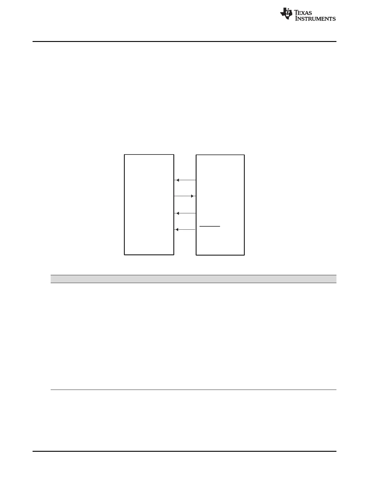
12.7.7 McBSP as an SPI Slave
An SPI interface with the McBSP used as a slave is shown in Figure 12-42. When the McBSP is
configured as a slave, DX is used as the SPISOMI signal and DR is used as the SPISIMO signal.
The register bit values required to configure the McBSP as a slave are listed in Table 12-17. Following the
table are more details about configuration requirements.
Figure 12-42. SPI Interface With McBSP Used as Slave
Table 12-17. Bit Values Required to Configure the McBSP as an SPI Slave
Required Bit Setting Description
CLKSTP = 10b or 11b The clock stop mode (without or with a clock delay) is selected.
CLKXP = 0 or 1 The polarity of CLKX as seen on the MCLKX pin is positive (CLKXP = 0) or negative (CLKXP =
1).
CLKRP = 0 or 1 The polarity of MCLKR as seen on the MCLKR pin is positive (CLKRP = 0) or negative
(CLKRP = 1).
CLKXM = 0 The MCLKX pin is an input pin, so that it can be driven by the SPI master. Because CLKSTP =
10b or 11b, MCLKR is driven internally by CLKX.
SCLKME = 0 The clock generated by the sample rate generator (CLKG) is derived from the CPU clock. (The
sample rate generator is used to synchronize the McBSP logic with the externally-generated
master clock.)
CLKSM = 1
CLKGDV = 1 The sample rate generator divides the CPU clock before generating CLKG.
FSXM = 0 The FSX pin is an input pin, so that it can be driven by the SPI master.
FSXP = 1 The FSX pin is active low.
XDATDLY = 00b These bits must be 0s for SPI slave operation.
RDATDLY = 00b
When the McBSP is used as an SPI slave, the master clock and slave-enable signals are generated
externally by a master device. Accordingly, the CLKX and FSX pins must be configured as inputs. The
MCLKX pin is internally connected to the MCLKR signal, so that both the transmit and receive circuits of
the McBSP are clocked by the external master clock. The FSX pin is also internally connected to the FSR
signal, and no external signal connections are required on the MCLKR and FSR pins.
 Loading...