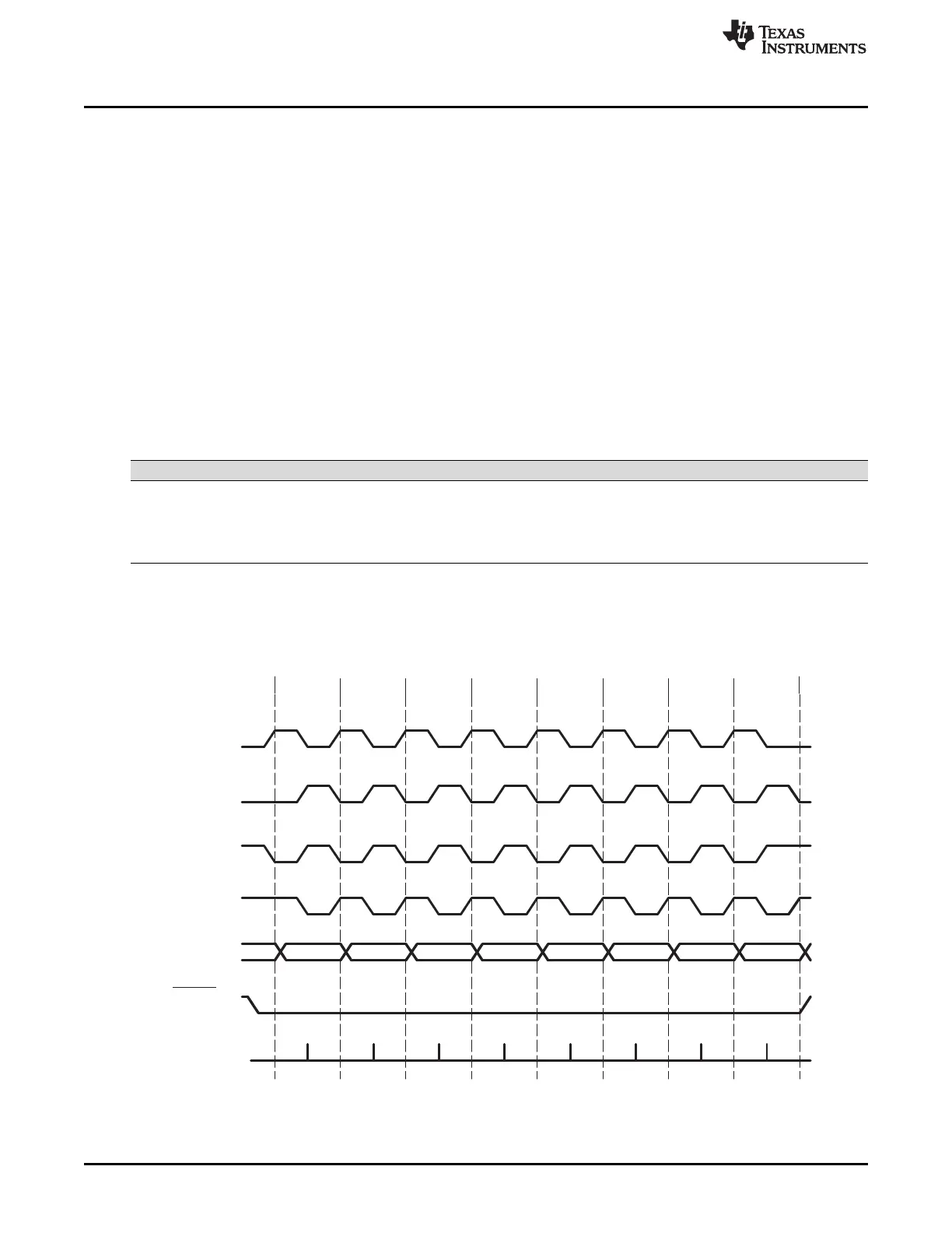
SPICLK cycle
number
1 2 3 4 5 6 7 8
SPICLK
(Falling edge
without delay)
SPICLK
(Falling edge
with delay)
SPISIMO/
SPISOMI
SPISTE
MSB LSB
Note: Previous data bit
(Into slave)
Receive latch
points
SPICLK
(Rising edge
without delay)
SPICLK
(Rising edge
with delay)
See note
SPI Operation
www.ti.com
558
SPRUI07–March 2020
Submit Documentation Feedback
Copyright © 2020, Texas Instruments Incorporated
Serial Peripheral Interface (SPI)
9.3.6 SPI Clocking Schemes
The clock polarity select bit (CLKPOLARITY) and the clock phase select bit (CLK_PHASE) control four
different clocking schemes on the SPICLK pin. CLKPOLARITY selects the active edge, either rising or
falling, of the clock. CLK_PHASE selects a half-cycle delay of the clock. The four different clocking
schemes are as follows:
• Falling Edge Without Delay. The SPI transmits data on the falling edge of the SPICLK and receives
data on the rising edge of the SPICLK.
• Falling Edge With Delay. The SPI transmits data one half-cycle ahead of the falling edge of the
SPICLK signal and receives data on the falling edge of the SPICLK signal.
• Rising Edge Without Delay. The SPI transmits data on the rising edge of the SPICLK signal and
receives data on the falling edge of the SPICLK signal.
• Rising Edge With Delay. The SPI transmits data one half-cycle ahead of the rising edge of the SPICLK
signal and receives data on the rising edge of the SPICLK signal.
The selection procedure for the SPI clocking scheme is shown in Table 9-3. Examples of these four
clocking schemes relative to transmitted and received data are shown in Figure 9-5.
(1)
The description of CLK_PHASE and CLKPOLARITY differs between manufacturers. For proper operation, select the desired
waveform to determine the clock phase and clock polarity settings.
Table 9-3. SPI Clocking Scheme Selection Guide
SPICLK Scheme CLKPOLARITY CLK_PHASE
(1)
Rising edge without delay 0 0
Rising edge with delay 0 1
Falling edge without delay 1 0
Falling edge with delay 1 1
Figure 9-5. SPICLK Signal Options
 Loading...