16
McBSP Receive
InterruptSelectLogic
MDXx
MDRx
ExpandLogic
DRR1ReceiveBuffer
RX
Interrupt
DRR2ReceiveBuffer
RBR1RegisterRBR2Register
MCLKXx
MFSXx
MCLKRx
MFSRx
16
CompandLogic
DXR2 TransmitBuffer
RSR1
XSR2
XSR1
PeripheralReadBus
16
16
16
16
16
RSR2
DXR1 TransmitBuffer
LSPCLK
MRINT
ToCPU
RXInterruptLogic
McBSP Transmit
InterruptSelectLogic
TX
Interrupt
MXINT
ToCPU
TXInterruptLogic
16
16 16
Bridge
DMA Bus
PeripheralBus
PeripheralWriteBus
CPU
CPU
CPU
Configuring Device Pins
www.ti.com
660
SPRUI07–March 2020
Submit Documentation Feedback
Copyright © 2020, Texas Instruments Incorporated
Multichannel Buffered Serial Port (McBSP)
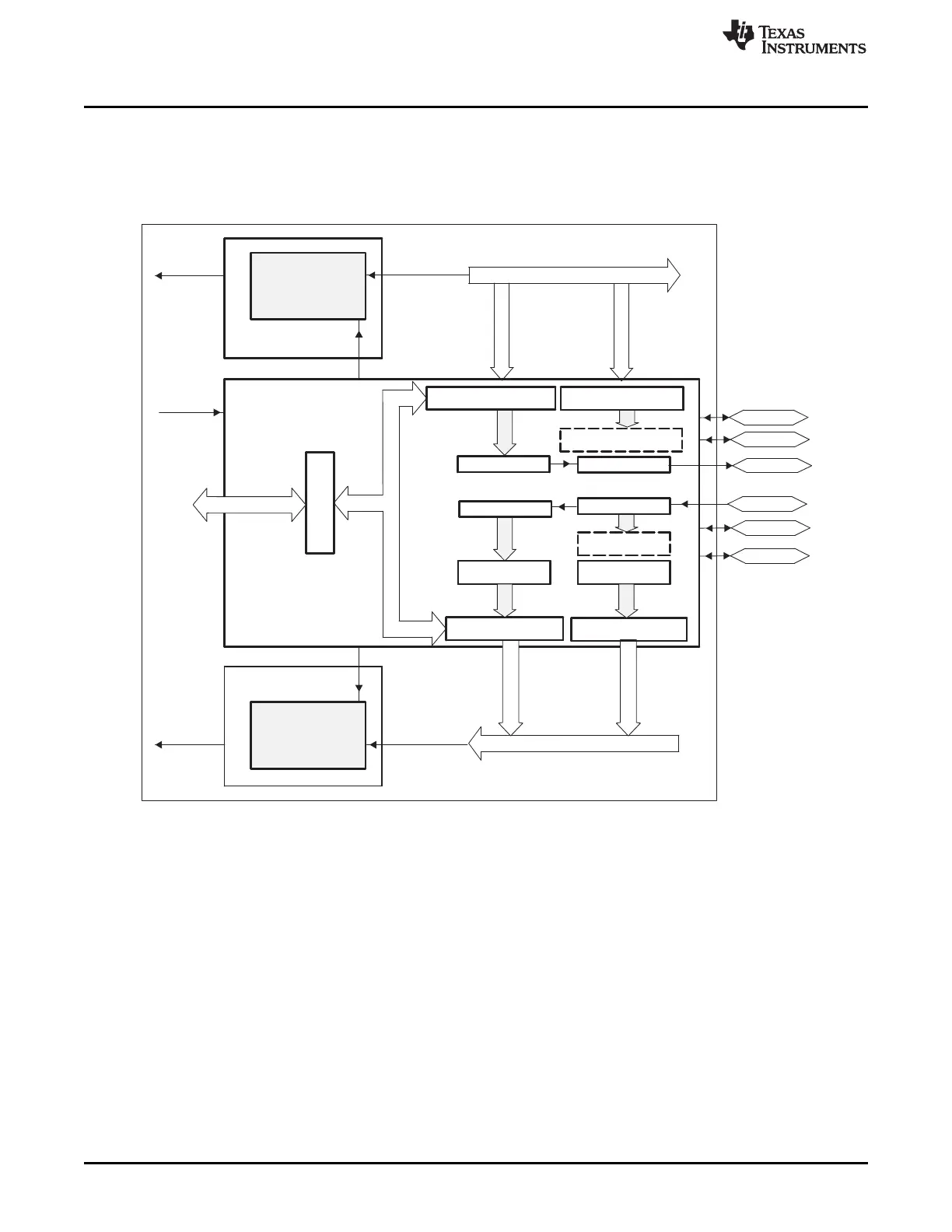
12.1.2.1 McBSP Generic Block Diagram
The McBSP consists of a data-flow path and a control path connected to external devices by six pins as
shown in Figure 12-1. The figure and the text in this section use generic pin names.
Figure 12-1. Conceptual Block Diagram of the McBSP
A Not available in all devices. See the device-specific data sheet
12.2 Configuring Device Pins
The GPIO mux registers must be configured to connect this peripheral to the device pins. To avoid
glitches on the pins, the GPyGMUX bits must be configured first (while keeping the corresponding
GPyMUX bits at the default of zero), followed by writing the GPyMUX register to the desired value.
Some IO functionality is defined by GPIO register settings independent of this peripheral. For input
signals, the GPIO input qualification should be set to asynchronous mode by setting the appropriate
GPxQSELn register bits to 11b. The internal pullups can be configured in the GPyPUD register.
See the GPIO chapter for more details on GPIO mux and settings.
12.3 McBSP Operation
This section addresses the following topics:
• Data transfer process
• Companding (compressing and expanding) data
• Clocking and framing data
 Loading...